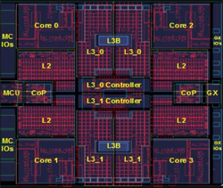
 The opening keynote of the 3D conference that I went to was by Subramanian Iyer of IBM. He described work they were doing on fully 3D chips for servers. The approaches I’ve already talked about don’t really work for the highest performance end of the spectrum.
Dramatic performance gains from architecture or pushing up clock rate are increasingly unlikely. Moving to a new process node brings performance gains but, of course, is enormously expensive. One of the remaining areas for improving system performance is increasing the size of the cache, and increasing the bandwidth of the cache/processor interface.
Flipping a memory over onto the processor is fine if the processor doesn’t need a heatsink. The highest performance server chips are now dissipating over 150-200W so they need to be on top. In addition, it is almost impossible to distribute the power across a chip like that. At 1V, 200W is 200A which you can’t even get into the chip through conventional wire-bond. And further, the dynamic fluctuations of processor load cause enormous voltage dips which eat up a lot of the potential performance if they are not eliminated.
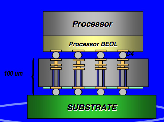
Using a silicon interposer to connect memory to the processor doesn’t work either since there is just too much long interconnect. The only solution is to build a true 3D chip with the processor on top, the memory underneath and with TSVs going through the memory die to carry all the power and I/O to the processor.
Although SRAM is faster than DRAM, DRAM is so much smaller and dissipates so much less power that in this setup it is preferable, not least because you can have a bigger cache (the memory and processor dice need to be about the same size). The small size wins back enough performance that it is a wash with SRAM.
 The picture to the right shows the basic architecture. On the top is the heatsinked processor die. There are no TSVs through the processor die. It is microbumped to attach to the memory die beneath it and to TSVs that go all the way through to carry the 200A of current that it requires direct from the package substrate. The processor/memory microbumps are at at a 50um pitch. The memory die to package bumps are 186um. The memory die has to be thinned in order to get the TSVs all the way through.
 In addition, the memory die is choc-a-bloc with decoupling capacitors to reduce transient voltage droops. This allows for increased processor performance without having to give up area on the processor chip for the capacitors since they are in the metal on the memory die. At the keynote, there was a video showing the dramatic difference to the voltage across the chip with and without this approach to supplying power.
