Global foundries’ plan for world domination

dr evilLast week I attended the Global Technology Conference, which sounds like something that the United Nations might sponsor but is, in fact, organized by Global Foundries.

Just in case you don’t remember who Global Foundries are, they are the old manufacturing arm of AMD which was spun out (partially, AMD still kept a share) and purchased by ATIC, a financial group based in Abu Dhabi. They since went on to purchase Singapore-based Chartered Semiconductor.

The first thing that surprised me about the conference was just how many people there were there, I’d estimate well over a thousand. There is clearly a lot of interest in the existence of a strong competitor to TSMC and Global seems to be the most likely candidate. They claim to be in the middle of the fastest volume process ramp for 40/45nm, using AMD’s microprocessor line as a yield driver.

Indeed, AMD announced two new microprocessors manufactured using Gobal’s 45nm node: Bulldozer and Bobcat.  Bulldozer is oriented to performance and scalability targeted at server farms. Bobcat is tailed for small die-size, low power targeted to portable devices. Both cores are complete re-designs.

A lot of Global’s strategy became clear from the presentations. They are clearly planning to be very aggressive at winning business at the 28nm and 22nm nodes. In fact I would go as far as to say they are “must win.” Abu-Dhabi may have deep pockets and are certainly investing freely, but eventually they will want to see serious profits coming back their way. They are investing a huge amount in process development and are building a big new fab (fab8) in Saratoga NY. They claim their process, which is high-K metal gate (HKMG) gate-first, is 15% more efficient that gate-last processes (take that, TSMC). But I’m not nearly enough of a process expert to have my own opinion. They are using ARM Cortex-A9 as a process driver, which they have already taped out. I’m guessing that because it is synthesizable, it is much easier to use as a process driver than an AMD design, which would otherwise be the expected choice.

Greg Bartlett, senior VP Technology and R&D, had some interesting perspective on what are the drivers of progress. Until about 60nm progress was almost all about improving lithography. That’s not to say that there wasn’t other development (copper interconnect, Hi-K dielectric etc) but the big breakthroughs were things like immersion lithography and double-patterning. Then a second driver came online, materials integration: strained silicon, HKMG. And from 32nm onwards 3D integration is going to be a 3rd big driver of value, driving density higher (although there are still some major power challenges to be addressed).

I was in a couple of meetings at DAC about 3D. One of the issues is the scale of the problem. There are a lot of separate problems that need to be solved from floorplanning (with multiple floors), simulating the entire stack of different interconnects, power and thermal analysis (and it’s not all bad, sometimes putting one die on top of another smoothes out hotspots since every die is also a heatsink), process issues (bumping etc) and all need to be solved pretty much simultaneously for it to be useful. It reminds me a bit of tape-automated bonding (TAB) which took much longer to come online than anyone expected for similar reasons. It’s hard to boil an ocean.


Posted in semiconductor | Comments Off

Polyteda

One startup I did run across that looks interesting is Polyteda. Let me first point out that this is all based simply on talking to them and I’ve not run their tools or done any other diligence.

They have a next generation DRC facing off against Calibre (also they have LVS). They are based out of the Ukraine. When I had a development group in Moscow when I was at Compass one of the things I noticed was that Russians thought differently (and yes, I know Ukrainians are not Russians). They had grown up in an era where the best computer you could expect was an old 286-based PC, you weren’t getting a state-of-the-art Sun workstation. Also, they grew up in an era where the Rouble wasn’t just not externally convertible, it wasn’t really internally convertible: you couldn’t buy stuff with it since it just wasn’t available. So they had a pride in doing a lot with a little, especially clever mathematics that just required a pen and paper, or processing large chips on inadequately powered computers. In addition, the Soviet universities were not seeded with American-educated professors, as was largely the case in India and China, so they were even educated differently from the rest of the world.

Polyteda is now qualified with UMC at 65nm, apparently the only DRC except Calibre since the others haven’t passed yet. While some are moving faster than others, it is safe to assume all of the foundries and many of the IDMs are at least investigating their technology if not actively working with Polyteda.

Polyteda takes a different approach to DRC, instead of being layer based, largely processing one layer at a time, it divides the chip up into areas and processes all rules on each area, fitting the whole thing in memory. They don’t overlap the areas (since that means double checking some things) so obviously this scales nicely to huge numbers of processors.

They have a much more programmatic way of expressing the design rules, including procedure calls, making for very compact rule-decks. Of course they can also read a Calibre deck but that is not a very efficient way of using the tools. Their language is more powerful, meaning they can check complex rules that other DRCs cannot, or can only do incredibly inefficiently: antenna rules, bizarre reflection rules, some stress rules and so on.

All other DRCs largely use scan-line algorithms, processing trapezoids as a line runs across the layers being analyzed. My guess is that they do not, that they instead do something closer to an approach I was shown back in those Compass Moscow days, following a polygon around from edge to edge and handling all the interactions. But that is pure speculation.

In this market, as Calibre showed at 0.35um, change can come fast. And since it is about a $400M market there is a lot of money up for grabs.

Posted in eda industry, methodology | Comments Off

DAC retrospective

So what was the theme of DAC this year? Two things stood out for me: one is that the big EDA companies are getting serious about doing design at a higher level. I think we need a new name for this since ESL tends to focus on IC design, whereas the underlying message is that moving to the higher level is about designing electronic systems including their software, not largely about chip design.Mentor has had a portfolio in this area for years. Synopsys has been vacuuming up companies at this level: VaST, CoWare, Synfora, Virage.

Cadence has put their EDA360 stake in the ground and also acquired Denali. I think the price is insane. John Bruggeman asked me whether I thought Virage or Denali was the better buy and I had to say Virage. I find it hard to believe that there is a huge untapped reservoir of demand for Denali’s products that the Cadence sales-force will unlock whereas I think the Virage product line can be leveraged by the Synopsys salesforce, especially given the rest of their IP portfolio. The interesting thing about the Virage acquisition is what, if anything, it does to affect their relationship with ARM since it now puts them squarely in competition with ARM for the old Artisan part of their product line, and, with ARC, at least obliquely in competition with them in the microprocessor space. But they both need each other so they probably just have to live with it.

EDA is still somewhat stuck in an outmoded style of design that assumes the chips are designed from scratch and then someone writes some software to run on them. In fact much of the software already exists: software generations are 10 times as long as chip generations, and chip design is increasingly about IP assembly rather than efficient design from scratch. I continue to believe that this block-level is an interesting choke point, with the potential to generate a virtual platform for the software developers and testers, and the potential to turn the design rapidly into an FPGA or SoC. But the tools don’t yet exist.

One other thing that is broken is clearly the funding model. There are very few new startups at DAC since VCs know that this is simply not an interesting industry: not growing, no IPOs and so on. Lucio Lanza, in his panel session, was pushing the notion that EDA software is going to become free, and open-source, and EDA companies need to make the transition to services like IBM. I don’t buy it. I don’t believe that open source will really work in EDA, at least at the leading edge, because open source has always proved poor at innovating products that require getting the specification right (and where the programmer is not the user). That’s the reason there are no good open source games. It is too hard to predict what will be a hit, and when a hit does come along it is too late to create an open-source clone. But EDA is a bit like that at the leading edge, with new process generations coming along. By the time you know the features you need in a tool it is too late to launch an open source project to clone it.

I was on a roundtable with Riko Radojcic of Qualcomm, and he pointed out that the big problems now are things like chip-package co-design, or software-power integration or complete 3-D design analysis, all areas that are probably too big for a traditional startup with an engineering team of perhaps 10 people max. But historically discontinuous innovation has always come from startups rather than the big established companies with less than a handful of exceptions. If the problems are too big, and/or the startups aren’t being funded, it’s not clear where the discontinuous innovation will come from.

I happened to be involved in couple of events where we talked a lot about 3D chip design: stacked die using various through silicon via (TSV) approaches to make the vertical connections. Javelin were working on this before their demise and Atrenta seemed to have picked the baton up off the ground. They had a demo working with imec and Qualcomm, along with AutoESL and Atrenta to demonstrate a 3D design flow, or rather the prototype for a design flow. What Riko calls pathfinding (hey, that’s very green recycling the name of the old Compass router) developing the outline for how to use a technology a couple of years before it is actually available. Qualcomm expect to do 3D production chips in 2012-3; so far they have only done test chips.

Of the companies I was working with, Oasys and Tuscany, both had essentially full suites the whole time.So although DAC felt quieter (see those extra-wide aisles) the key people seemed to be there. It remains a weird show, largely put on for the key purchasers in a few dozen companies.

Oasys had irreverent videos taking off the “I’m a Mac, I’m a PC” ads. Synopsys people (even Aart) would sneak by trying to get a peek without actually blatantly standing there and looking. They are pretty funny, and are now up on the Oasys website.

Next year, DAC is in San Diego from June 5-10th.

Posted in eda industry | Comments Off

Linaro: the latest in the ARM and Atom battle

Usually when two companies initiate a joint venture or work together, it is often casually referred to as the two companies getting in bed together. Last week, a veritable orgy was announced. ARM, Freescale, IBM, Samsung, ST-Ericsson and Texas Instruments announced that they are creating a company, Linaro, to provide better distribution and tools for Linux.

Reading between the lines, this looks like it is all going to be ARM-based. The first release is optimized for ARM’s Cortex-A family, the quote in the release is from ARM’s VP of corporate development, and all the companies in the announcement have significant investment in ARM-based products.

Traditionally Linux has been developed to run on Intel processors. It was originally “Unix for the PC.” Because of architectural compatibility this meant that Linux ran on Intel’s Atom core too. This consortium is going to try to make sure that Linux runs even better on ARM-based platforms. None of these semiconductor manufacturers can ship products for smartphones and netbooks without a good Linux release. On the other hand, by pooling their resources they will end up with a software stack at a fairly low cost and zero marginal cost. They are not going to compete on the OS level of the software stack.

But therein lies a problem for them. If the software stack is the same for everyone, it is very hard to differentiate much on the hardware level underneath either. Yes, performance and power consumption will be differentiators but using the same ARM cores on similar silicon means the differences will be minor. Which leaves price.

First Apple and then Google’s strategy in wireless has been to put all the differentiation in application software and industrial design, reduce the wireless network operators to dumb pipes (no more walled gardens) and reduce the hardware suppliers to commodities (all Android phones are pretty much the same).

On the same day, AT&T announced that it was ending unlimited data plans that has been one of the big drivers of mobile Internet. But they obviously don’t think that they are making enough money as a dumb pipe to justify the infrastructure costs. Apparently a tiny handful of users generate almost half the data traffic, although the limits of 2 GB seem unnecessarily low if there really are such a small number of superusers who are overloading the network.

So this is the future: commodity chips going into commodity phones running a commodity operating system on a commodity wireless network. The money is in what you do with your phone, just as it is in the non-mobile world.

I think that for the time being, Apple will be able to command a higher price point and some differentiation but their costs will be much higher and that might eventually become a big problem. But in the meantime they will make all the money.

Posted in semiconductor | Comments Off

Design Automation Conference preview

Unless you have been hibernating through the winter (which some days seems to still be going on) then you know that DAC is coming up on 13th June through Friday if you stay all the way through the tutorials.

So what’s new this year?

The DAC party has moved from Wednesday to Tuesday, and is now sponsored by Denali. This is not to be confused with the Denali party itself, which is now on Monday night (and, remember, you must register at their website to get a “ticket,” actually a wristband if history is any guide, or you will not get in). And in this compressed world, Cadence has an event for press and bloggers; Mentor has an event for press and bloggers; and Synopsys has an event for anyone connected with their system portfolio. All of these events are early Monday evening. It looks logistically impossible.

The exhibits are no longer free. Atrenta, Denali, and Springsoft created the “I love DAC” movement to sponsor 500 free exhibit passes. But they’ve all gone. So if you don’t have one, your initiative test is to find an EDA vendor who you know well enough to get you in. Or become a blogger and you count as press.

Also on Monday, Ed Sperling is hosting a discussion on “What’s broken in EDA?” at 11am and I am one of the participants. Not sure where yet. But you know that this is a subject that I can talk about for longer than anyone would want to listen.

On Sunday, in previous years, there has been a long Workshop for Women in Design Automation that you had to pay to attend. Although formally not restricted to women (probably not legal anyway) it was basically attended by, yes, the women in EDA.

This year’s recipient of the woman of the Marie Pistilli award is Mar Hershenson. Now at Magma, she is perhaps most well known for being the founder and CEO of Barcelona Design, a company in the analog IP space that never quite got traction. She then founded Sabio Labs and sold it to Magma.

But the big change is the format of the Women Workshop has now changed to be a DAC 2010 Career Workshop, and men too are encouraged to attend (hey, we have work-life balance issues and other things like that too). The keynote speaker is Patty Azzarello, author of a new book “Off the Org Chart” about taking control of your career. Two other big changes are that the workshop is now much shorter, from 11.30am to 2pm, so no longer requires the investment of most of a day. Plus, it is free thanks to the sponsorship of Atrenta, Axiom, Cliosoft, Eve, Jasper, Mentor, MP Associates, Real Intent, SpringSoft, and Synopsys. However you must pre-register for it to get in free.

Posted in eda industry | Comments Off

EDAgraffiti, the book

edagbook.jpgThe book of the blog is now available for purchase here. Here’s an extract from the introduction that gives an overview of what the book is:

This book is an outgrowth from this blog. Although the basis of the book is the original blog entries there is new material and the old material has been extensively revised. Furthermore, I’ve reordered the content so that each chapter covers a different area: Semiconductor, EDA marketing, Investment and so on.

I’ve tried to write the book that I wish I’d been able to read when I started out. Of course it would have been impossible to write back then, but in a real sense this book contains 25 years of experience in semiconductor, EDA and embedded software.

Not many books cover as wide a spectrum of topics as this. I’ve ended up in marketing and executive management but I started out my career in engineering. For a marketing guy I’m very technical. For a technical guy I’m very strong on the business and marketing side. It is an unusual combination. I started in semiconductor, worked in EDA but also in embedded software. I’m a software guy by background but spent enough time in a semiconductor company that I have silicon in my veins.

I certainly won’t claim that this is the only book you need to read, so the end of each chapter has a “bookend” that looks at one or two books that are essential reading for that area, a taster to encourage you to read the book yourself.

There are a few threads that recur through the whole book, leitmotifs that crop up again and again in widely different areas.

  • Moore’s Law, of course. But really something deeper which is that semiconductor economics, the fact that transistors have been constantly getting cheaper, is the key to understanding the industry.
  • Software differentiation. The reality is that most of the differentiation in most electronic systems is in the software (think iPhone).
  • FPGA-based systems. Combining these two trends together, chips are getting too expensive to design for most markets so “almost all” designs are actually software plus FPGA or standard products.
  • Power is the limiter in many designs today. We will be able to design big systems but not be able to power up the whole chip at once.
  • Multicore hits all these trends. Nobody really knows how to write software for multicore designs with large numbers of cores, nor how to handle the power issues.
  • Finally, all the major breakthrough innovations in EDA have come from startup companies, not the big EDA companies. But the exit valuations are so low that no investment is going into EDA startups so it is unclear where the innovation will come from going forward.

The book is available for purchase here. If you are interested in buying in bulk (makes a great giveaway for your best customers at DAC, or for your user-group meeting, or for your sales kickoff) then contact me directly. I can also put a special cover on it with a company logo.

Posted in admin | Comments Off

Cadence summits Denali

denali.jpgCadence announced that they had acquired Denali for $330M today. They reckon that it will be accretive this year. Since the beginning of the year there has been a sort of land grab going on in the system and IP spaces. There are rumors around that at least one of the high-level synthesis companies is about to be acquired too.

It is going to be interesting to see just how this all plays out. Magma isn’t playing this game, they are sticking to IC design for now.

Mentor is the market leader in high-level synthesis (HLS) with their Catapult product, and they have had an embedded software and RTOS business for many years. However, they have no virtual platform technology. Mentor also has a strong PCB offering, another important part of design once you get up off the raw silicon.

Cadence has a relatively new HLS product, CtoSilicon, they have a partnership with Wind River (Virtutech) around Simics for virtual platform (although this is brand new so too soon to tell how it will work out) and have had no IP portfolio to speak of until today’s Denali acquisition. I’m guessing that Synopsys would have been interested in Denali but didn’t want to pay that much. Cadence also has a strong PCB design offering.

Synopsys has no HLS product, although rumored to be in discussion to acquire one. They have Virtio, VaST and CoWare in the virtual platform space. And they have the strongest IP portfolio of any of the big companies. However, they have no offering in the PCB space.

It is going to be interesting to see how this plays out. The problem for all the EDA companies is that as you move up to higher levels of design, then “almost all” designs are FPGA-based and do not involve designing a special ASIC/SoC/ASSP. This does not play to these companies strengths. For the FPGA/embedded market their channel is simply too expensive and doesn’t call on the right accounts. When I was at Cadence, their system design tools were in a separate organization, the Alta Group, which had its own sales team. The business was growing nicely. Cadence decided to optimize expenses and roll the Alta Group back into Cadence proper and take away the separate sales team. From that point on their products pretty much went into decline and eventually Cadence transferred them to CoWare in a deal involving transferring the team, getting royalties, taking some stock and maybe even some real money (so amusingly those CoWare businesses are now part of Synopsys and presumably Cadence got some money out of the deal for their share of CoWare).

It will be interesting to see if any of the big 3 EDA companies bites the bullet and puts its system strategy into a separate organization with its own channel and, perhaps, logo. I have a feeling that it will be a necessary condition for success once a critical mass of products exists. As I said about Cadence’s EDA360 announcement, real success will be if Cadence is selling significant product to companies which are not doing IC design. The same goes for Mentor and Synopsys.

Posted in eda industry | Comments Off

Is it time to start using high-level synthesis?

autoesl.jpgOne big question people have about high-level synthesis (HLS) is whether or not it is ready for mainstream use. In other words, does it really work (yet)? HLS has had a long history starting with products like Synopsys’s Behavioral Compiler and Cadence’s Visual Architect which never achieved any serious adoption. Then there was a next generation with companies like Synfora, Forte and Mentor’s Catapult. More recently still AutoESL and Cadence’s CtoSilicon.
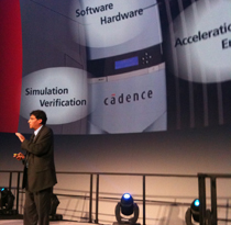
I met Atul, CEO of AutoESL, last week and he gave me a copy of an interesting report that they had commissioned from Berkeley Design Technology (BDT) who set out to answer the question “does it work?” at least for the AutoESL product, AutoPilot. Since HLS is a competitive market, and the companies in the space are constantly benchmarking at customers and all are making some sales, I think it is reasonable to take this report as a proxy for all the products in the space. Yes, I’m sure each product has its own strengths and weaknesses and different products have different input languages (for instance, Forte only accepts SystemC, Synfora only accepts C and AutoESL accepts C, C++ and SystemC).

BDT ran two benchmarks. One was a video motion analysis algorithm and the other was a DQPSK (think wireless router) receiver. Both were synthesized using AutoPilot and then Xilinx’s tool-chain to create a functional FPGA implementation.

The video algorithm was examined in two ways: first, with a fixed workload at 60 frames per second, how “small” a design could be achieved. Second, given the limitations of the FPGA, how high a frame rate could be achieved. The wireless receiver had a spec of 18.75 megasamples/second, and was synthesized to see what the minimal resources required were to meet the required throughput.

For comparison, they implemented the video algorithms using Texas Instruments TMS320 DSP processors. This is a chip that costs roughly the same as the FPGA they were using, Xilinx’s XC3SD3400A, in the mid $20s.

The video algorithm used 39% of the FPGA but to achieve the same result using the DSPs required at least 12 of them working in parallel, obviously a much more costly and power hungry solution. When they looked at how high a frame rate could be achieved, the AutoPilot/FPGA solution could achieve 183 frames per second, versus 5 frames per second for the DSP. The implementation effort for the two solutions was roughly the same. This is quite a big design, using ¾ of the FPGA. Autopilot read 1600 lines of C and turned it into 38,000 lines of Verilog in 30 seconds.

For the wireless receiver they also had a hand-written RTL implementation for comparison. AutoPilot managed to get the design into 5.6% of the FPGA, and the hand-written implementation achieved 5.9%. I don’t think the difference is significant, and I think it is fair to say that AutoPilot is on a par with hand-coded RTL (at least for this example, ymmv). Using HLS also reduces the development effort by at least 50%.

BDT’s conclusion is that they “were impressed with the quality of results that AutoPilot was able to produce given that this has been a historic weakness for HLS tools in general.” The only real negative is that the tool chain is more expensive (since AutoESL doesn’t come bundled with your FPGA or your DSP).

It would, of course, be interesting to see the same reference designs put through other HLS tools, to know whether these results generalize. But it does look as if HLS is able to achieve results comparable with hand-written RTL at least for this sort of DSP algorithm. But, to be fair to hand-coders, these sort of DSP algorithms where throughput is more important than latency, is a sort of sweet-spot for HLS.

If you want to read the whole report, it’s here.

Posted in methodology | Comments Off

Around the Imax with EDA360

e360.jpgCadence had a big announcement at the Embedded Systems Conference this week. Actually, not at the conference (I don’t think they even have a booth) but in the Imax theater in the Tech Museum (and, on another topic, are they ever going to update any of the exhibits in the Tech Museum?) Yes, Cadence and embedded systems are not things you usually think of together. However, they announced their vision for the future of EDA, which they call EDA360.
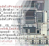
The EDA360 vision is actually pretty close to a lot of the themes that I’ve talked about on this blog: the increasing irrelevance of chip design in the much bigger universe of electronic system design, the growing importance of software and so on.

For Cadence to move up to the system design level they lack a number of things. Firstly, they have no virtual platform technology to provide to the software developers. They do have high level synthesis, the CtoSilicon (curiously Synopsys is the one that doesn’t but I expect them to buy one of the existing companies, if not immediately then whenever it is clear who the winner in the space is). They don’t have FPGA synthesis, which is a problem since most designs are FPGAs. And they don’t have anything for the embedded software space. Of the big EDA companies, only Mentor has although they’ve struggled to grow it as much as they’d like.

Cadence also announced a couple of specific programs. The first is an attempt to plug the virtual palatform hole: a partnership with Wind River around Simics (the software from Virtutech that Intel/Wind River acquired earlier this year). If that’s Cadence’s strategy I’m not sure why they didn’t buy Virtutech (reputedly they tried to by CoWare for nearly $100M and Virtutech sold for only $45M).

The other thing they announced was the Cadence Verification Computing Platform. I’m not 100% sure what this is. I think it is the latest product in the Quickturn line of accelerators and there was certainly an impressive looking box among the wine and appetizers. But in an attempt to position this as the second significant step in EDA360 they layered it with so much marketing smoke that you couldn’t see through to the mirrors.

EDA360 is a four-legged stool. The basic premise is that there is a tectonic shift going on in the semiconductor industry. Instead of just delivering systems they need to deliver a complete value stack with a lot of software too. I still think that one of the big challenges there is that semiconductor companies only know how to sell margined up square metres of silicon, and treat software as a marketing expense. That was fine when there was only a bit of it, but when there is more engineering effort in the software than the chip, and a lot of the differentiation is in the software then this is inappropriate. So leg number one of EDA360 is that there needs to be a shift towards focusing semiconductor companies more on integrating hardware and software IP, and less on design creation, in order to get their profitability up.

The second leg is application-driven system realization. I think this is close to what I call software signoff. Instead of developing a chip and then worrying about writing some software to run on it, conceptually it is the other way around. The software comes first and the only purpose of the hardware (which may or may not be a chip) is to run it fast enough, and at low enough power, and provide the required interfaces to the outside world (wireless, 3G, optical etc). From a practical point of view, though, it is not enough just to provide the hardware since a lot of software may well be provided by the end-user. So the software ecosystem must be fed with drivers, development kits, simulators and so on. Think of what Apple provides for iPhone developers.

The third leg is software-aware SoC realization. I think this is really a subset of the second leg for designs where the system is actually (mostly anyway) a single chip. SoC design, of course, is Cadence’s comfort zone. But tying into software really increases the importance of transaction-level modeling, virtual platforms, and generally realizing that the software is often master over the chip design requirements.

The fourth and final leg of the EDA360 stool is silicon realization. This needs to be made more efficient by pushing up the level of abstraction, building appropriate links up to the software world (especially for power consideration) and so on. This is sustaining and updating the existing product line in a way that Cadence would have had to do anyway.

I think Cadence is trying to go in the right direction and it will be interesting to see what specific things they do to flesh out the vision with real products. One of the big challenges is that their focus and revenue comes mostly from IC design, moving up into the system space is disruptive (in the Innovator’s Dilemma sense). I think success would be when Cadence is making serious money selling to people who do no chip design, just build systems with FPGAs, boards and standard products (plus lots of software). The challenges are largely on the business side rather than the technology side. As the old joke about a guy asking for directions in rural Ireland goes, “If I were you, I wouldn’t start from here.” It’s not clear whether Cadence’s IC heritage is the right base upon which to build this vision.

Posted in eda industry, marketing | Comments Off

EmbeDAC

embedded.jpgThe latest EDAC spring meeting was a bit different from usual. The panel session was all about embedded software. John Bruggeman, now at Cadence but previously at Wind River, lined up his old colleague Tomas Evensen (the CTO of Wind River, now part of Intel), Jim Ready (the CTO of Montavista, now part of Cavium Networks) and Jack Greenbaum (director of embedded software engineering for Green Hills Software, still independent).

Jack started off the proceeding by pointing out that for most designs the software engineering costs more than the IC engineering. For him the business drivers were 16 bit designs all going to 32 bit, 32 bit designs going to 64 bit, multicore and virtualization (using a single core to run code binaries from what used to be several separate microprocessors). Tomas added the drive towards open source. And Jim emphasized the thrust of Linux into embedded.

Tomas talked a bit about why Intel had acquired Wind River and why they had also left it to remain independent. To ship a chip these days you need to ship it with a state-of-the-art software stack, so Intel wants to ensure that for its products. But unlike previous acquisitions, such as Freescale (then still Motorola) with Metroworks, Intel didn’t want to kill the ecosystem and devalue the software by taking everything in-house and making it Intel specific.

Everyone complained about the challenge of getting people to pay for software. In the IC world nobody would dream of trying to design a chip without software, or even writing all their own software. In the software world people won’t make the investment even if the ROI is there. So system companies place tremendous value on software but refuse to pay, and silicon provides less value but gets all the revenue.

Everyone thought partly that this was due to people not taking quality seriously. Apparently 40% of cars taken into dealers involve a re-flash of an ECU (electronic control unit) because the initial and ongoing quality is so poor. Perhaps the current woes at Toyota will cause a re-think on whether it is appropriate to invest for software quality.

Quailty is expensive. DO-178B (a standard for certifying avionics) costs $1000/line to validate. Meanwhile car companies are worrying about the number of resistors on the PCB. Quality will only happen when companies decide it is worth the money. Tomas talked of a system he was involved with that was validated. Since the early 1990s not a single bug has been found in it. And Jim boasted that he was involved at Ready Systems in 4K bytes of avionics code that was the first certified.

Tomas and Jim both emphasized that despite Linux being open-source it was still a viable business. Montavista has shipped over $250M of “free” software. But one cloud was that Android drives out differentiation and so squeezes vendors. It even marginalizes the hardware since it is now very generic.

The DNA of EDA and embedded software are very different. EDA is dominated by physics but software is dominated by psychology. So before EDA ventures into the software world it needs it understand it deeply since analogies don’t carry across.

This was brought home when Gary Smith asked about what they were going to do to write power-aware software. Everyone just took this as being a question about battery life rather than realizing that the big problem is going to be having a chip that we can’t light up all at once. It would help, of course, if the chip people added circuitry to make it easy for the software to monitor power, today’s chips rarely even have cache-miss counters which is one of the biggest contributors to power.

Power may turn out to be the thing that finally ties the software development process to the chip development process, since it will become impossible to develop software without worrying about it. It will even affect software architecture, not just detailed low-level stuff.

Posted in embedded software | Comments Off