Ticonderoga

When I was at Cadence, one of my jobs was to be the technical interface to investors and analysts. The finance organization, with its investor relations department, could handle all the numbers but if anyone wanted to talk about technology then I was the person that got called in. I knew enough about the technology across the whole product line to be credible, and I was house-trained in what I could and could not say to investors. If you ever have to spend any time talking to investment analysts or the press then you know that they will try and get you to reveal things that are coming down the pipe. Here’s  the phrase to drill into your brain to bring out on autopilot at such times. It firmly says nothing without being rude: "We have no announcements to make at this time."

One of the analysts back then was Jay Vleeschhouwer (I bet you leave out one of the "h"s if you type his name without looking) who was at Merrill Lynch until the recent downturn. He was one of the most technical of the analysts that covered EDA and so I spent a fair bit of time with him. He’s resurfaced at Ticonderoga Securities. I had breakfast with him a couple of weeks ago. He’s just finished a big more-than-you-want-to-know report on the EDA industry that is 55 pages long. Ticonderoga have announced that they are initiating EDA coverage (plus coverage of some other software companies). Their (Jay’s) initial stock recommendations are Cadence neutral, Mentor buy and Synopsys neutral. Remember that a good rule of thumb about recommendations is to back them all off to be more negative. So phrase like "strong buy" means "buy", "buy" means "hold", "neutral" means "don’t buy", "hold" means "sell" and "sell" means "you stupid idiot why didn’t you sell this dog ages ago."

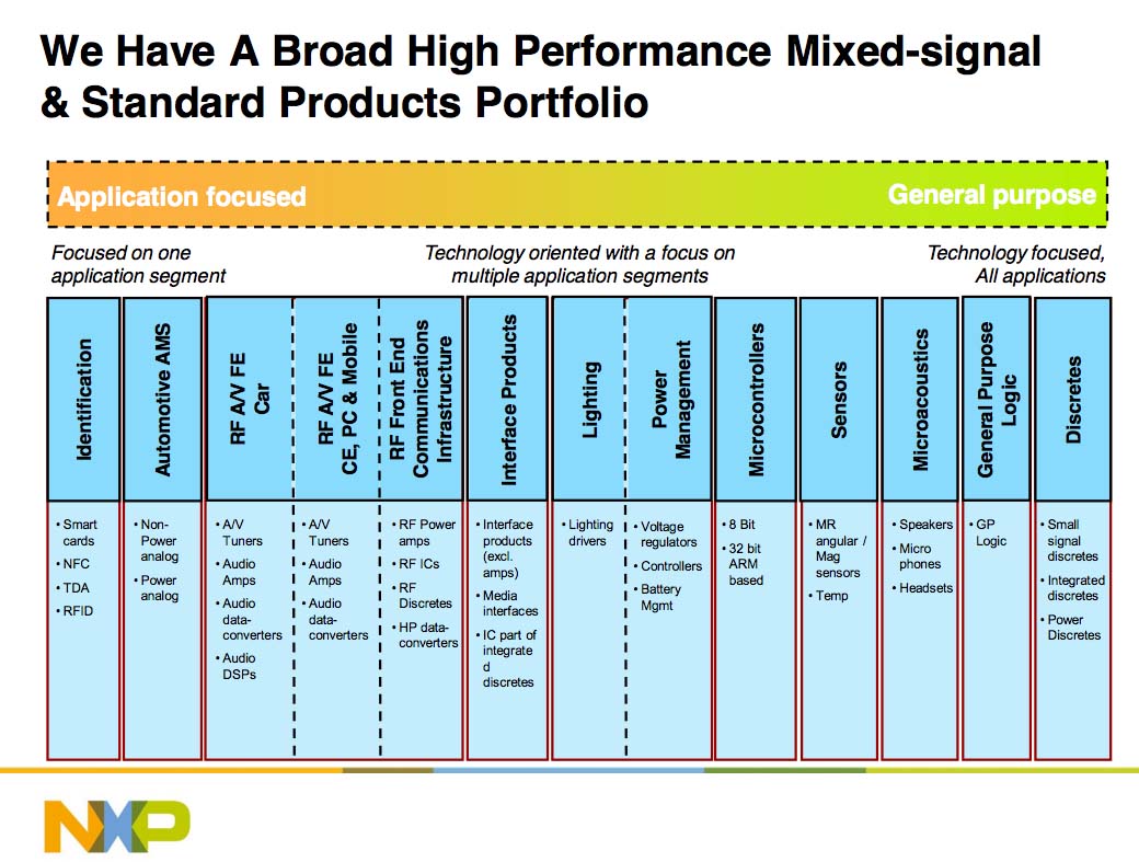
Jay estimates that EDA declined by 10% in 2009 to $4.15B after a previous 11% decline in 2008. He’s forecasting growth of 3-4% in 2010 (although this is misprinted as 2011 in the summary but not the body of the report).

I love all the boilerplate risks that SEC rules now kind of make necessary: Risks include better or worse than expected industry conditions; better or worse than expected bookings and product adoption; better or worse than expected share gain; better or worse than expected margin leverage; or better or worse than expected cash flow. In other words, I could be wrong. Jay will also be moderating the EDAC CEO forecast panel later this month, where we can expect Wally to produce lots of quantitative graphs showing how good or bad 2010 will be, Aart to say that Synopsys is in their quiet period so he can’t say much, and Cadence to predict that 2010 will be better than 2009 since it could hardly be otherwise.

Posted in investment | Comments Off

Consumer Electronics Show

At the start of January I went to the Consumer Electronics Show (CES) in Las Vegas. It is quite unlike any trade-show I’ve ever been to before. It fills all the halls of the Las Vegas convention center plus a hotel or two. There were 130,000 people attending. For comparison, AT&T park has a capacity of 41,000 so it is about 3 times as large. And if you think the traffic is bad after a ball-game you can try 2 hour waits for taxis and even 30 minute waits for the monorail (it runs every 5 minutes or so but it takes 4 or 5 of them before you get to the front of the line).

DAC is the tradeshow I know best. I’ve been to every one since 1984, the year DAC got big and Albuquerque was still small. I’ll probably still be going when DAC is small again. Anyway, unlike DAC, you can’t just wander around hoping to run across the interesting stuff. There are so many booths you can’t hope to see more than about 20% of them even in a couple of days. You have to decide which people you want to see and fight your ways through the mêlée to their booths.

One company, actually an $800M semiconductor company, we met with simply didn’t bother to have a booth. They just rented a suite in one of the nearby hotels and had all their meetings there. It was actually much easier to find them than if they had had a booth. But we were ravenous during the meeting. Unless you have 45 minutes to stand in line you aren’t getting any lunch. We tried to crash an NXP special event with a buffet but the security guard got to us first.

In EDA, many people wonder about the future of tradeshows. DAC seemed fine this year but it was on home turf. It will be interesting to see how it does in Anneheim this year where most visitors have to get on a plane rather than just get into their car. But CES seems to have had more visitors than they predicted. But for really big tradeshows the end can come fast if the biggest guys pull out. Remember Comdex, which was also one of the largest tradeshows anywhere with 200,000 attendees. Hotel rooms went for several thousand dollarsd per night. Comdex died in 2003, ironically partly because the center of gravity for computers had moved so far from being in the IT departments of corporations to consumers, and CES became the must-attend show.

Posted in security | Comments Off

One year on

It is the one-year anniversary of Obama’s inauguration and so I decided I’d look back at the blog entry that I wrote a year ago to see how well it has stood up. I called out a couple of big things that I worried were likely to happen in the Obama administration with its control of both houses.

The first was that success would be decided in Washington through lobbying and rent-seeking rather than the marketplace. Of course, Washington doesn’t control the entire economy but there has been no shortage of examples to point to of this. Government picking winners never seems to work. I lived in Britain in the 1970s and saw plenty of that then. The big problem is that the government doesn’t pick winners, they pick losers who happen to have strong political power; dying or mismanaged companies like GM or Fannie-Mae or Citibank. I don’t think we want the government trying to pick winners like some sort of venture capitalist of last resort looking for the next Google, but it would probably be a better use of the money. I saw an interesting analysis the other day that the entire space program of the 1960s to put a man on the moon, adjusted for inflation, cost less than the AIG bailout. Of course the country is richer now, even in the downturn, than it was then so it may be less as a percentage of GDP, but still.

The second thing I worried about was anti-trade rhetoric. Semiconductor and EDA are global businesses, since you can’t really build a fab and just serve the local market from it; they are too expensive. I think there is probably some sort of trade-war coming with China, partially because they will make a good scapegoat during the elections later in the year, and partly because China really is a lot less open to trade than they try to appear. And it will hit the news soon since the WTO has accepted to hear China’s complaint about the US tariff on cheap tires. It is also going to be interesting to see how the latest spat with Google plays out. Further, since most of Asia pegs its currency to the US dollar, and the US dollar is weak due to the unending deficits, it can only decline in practice against the European currencies, which will lead to trade tensions there too as European exports to Asia and the US become increasingly overpriced.

The best thing for Silicon Valley is when the marketplace picks winners and losers and Washington keeps out of the game. Brown’s election in Massachusetts is a warning shot across the bow of the current administration but I don’t think it is any kind of endorsement of the Republican party policies—does anyone even know what they are? Until today the Republican strategy for the 2010 elections seemed like it would be to run on the policy of repealing an unpopular health-care bill. Now they’ll actually have to say what they might do instead.

Posted in silicon valley | Comments Off

Shake that EDA malaise

I have a sort of op-ed piece in Electronic Design today. Anybody who has been following my musing here (and, yes, I know I’ve not mused very much recently; must muse more ) won’t be surprised by anything I say.

The piece ended up being headlined “To Shake Its Malaise, EDA Must Look To Where Design Is Really Happening.” Journalists are constantly complaining about bad headlines being attached to their wonderful work, but in this case I think that the headline is a good summary of what I say.

The bottom line is that EDA, focused as it is on IC design in advanced processes, is focusing on a decreasingly important part of the overall electronic design process. Yes, you can’t design a leading-edge chip without EDA so the market isn’t going to go away. But most electronic systems use off-the-shelf chips rather than designing them from the ground up. There will always be a market for bespoke Saville Row tailoring of expensive suits, but the real market is at Macy’s, Nordstrom’s and Mens’ Wearhouse.

Here’s an example. The biometric company I work for has a fingerprint-protected USB drive product (that we got working the night before CES, it’s not just taping out a chip that comes down to the wire). It contains some flash memory, a USB and hardware-encryption chip (standard product) and a programmable Luminary chip (now part of Texas Instruments). The whole system requires a fingerprint sensor and an OLED too, which obviously can’t be integrated onto a custom chip in any case. Of course in volumes of hundreds of millions it would make sense to integrate the Luminary chip (which is an ARM processor with some standard peripherals) and the USB/encryption chip. But it will never ship in those volumes (I can dream) so I can’t imagine that would ever make sense. Although, as a long-term IC guy, it upsets my sense of elegance to have two chips that clearly “should” be integrated, it is simply cheaper to use two separate chips. Most electronic products are like this: a handful of highly-integrated but standard chips on a little circuit board.

One theme that runs through this blog is that semiconductor economics drives everything. Semiconductor is a mass-production process that can deliver very cheap chips but only if the “mass” in mass-production is large enough. Otherwise the fixed costs overwhelm: the cost of design, the cost of masks and the fab setup times. The only alternative is to aggregate end-user systems so that the same chip is used in multiple designs. FPGAs are obviously one form of aggregation, just buy raw gates and put them together later. The Luminary chip in the Biogy drive is another.

I certainly don’t claim to have all the answers as to what the big EDA companies should do. But somebody needs to be the Mens’ Wearhouse of EDA and serve the mainstream market, even though the unit price is lower. I guarantee it.

Posted in eda industry, silicon valley | Comments Off

The fleas aren’t doing so badly

Way back in the mists of time early last year, at the EDAC CEO forecast panel, we were asked to forecast the stock prices of Cadence, Mentor, Magma, MIPS and Synopsys. See "we are fleas on a sick dog."

I went back and looked at my predictions. I forecast (well, guessed would be a more accurate verb) that Cadence would be 6 (up from 4), Mentor would be unchanged at 5, Magma would have been taken private, MIPS would have been acquired and Synopsys would have declined to 15 from 18. The stock market for the year has been much stronger than I would have forecast which means that I was being too pessimistic.

Well obviously Mamga didn’t go private (its stock is 2.31 today, way up from its low for the year of 0.68). MIPS is still hanging on as an independent company (its stock is 4.37, also way up from its low for the year of 1.04). Mentor gradually climbed up for much of the year and ended up at 8.83. Synopsys went up, not down as I forecast, and ended up at 22.28.

But Cadence came through for me. I predicted 6 and they obligingly ended the year at 5.99.

Posted in eda industry | Comments Off

Cadence goes two-dimensional

Yesterday I spent an hour with John Bruggeman, who has now been CMO at Cadence for just over a couple of months. As I’ve said before, I knew John before he joined Cadence since he was the CMO for Wind River during the time I was VP marketing at Virtutech, both of us in the embedded space. One thing I didn’t know was that John was at Oracle when, nearly 20 years ago, they decided to move from being focused on technology (our relational technology is better than yours) to tying their technology into the business processes of their customers.

John’s view is that EDA has been driven entirely by the need to make designers more productive. My own view is that everything comes back down to semiconductor economics, but the arguments may basically be the same. If we got back several process generations where the issues where clearer, we find that the move from, say, 0.5um to 0.25um was driven by the fact that a 0.25um chip was no only faster and lower power than the 0.5um one, it was about 50% of the cost per transistor. So even if you were quite happy with 0.5um you had to move anyway. But each process generation brings new challenges, not least that chips get bigger all the time, so the EDA tools and methodologies need to improve designers’ productivity enough to keep up. This, in turn, drove EDA companies’ revenues.

Looking a little deeper, the EDA companies would work with the leading edge early adopters of each new process generation to produce the tools required for success. There wasn’t that much money in the new process generation at this point, too few designs were being done in the new node. Eventually the leading edge would move to the next node, and the mainstream would come through as a sort of cash-cow. Engineering had already moved on, but the previous node tools could be sold in high volume for significant revenue.

This model is somewhat broken now. Semiconductor economics means that only the highest volume chips can justify doing a design at 45nm or 32nm. Semiconductor is a mass-production technology and the mass required for economic viability of a chip goes up at each process node. In turn this means that the mass market that made the EDA business grow is not coming through and so not driving revenue in the same way. Of course there are still designs going on in 90nm and 130nm but, by and large, everyone has all the tools they’ll need already.

John told me that obviously Cadence will continue to push on the productivity strategy. After all, Cadence’s bread and butter is ensuring that the leading edge semiconductor companies can design leading edge chips successfully.

But John wants to have a two-dimensional strategy, where the other dimension is profitability. Design tools potentially generate an incredible amount of data. After all, every button click, every file write, every verification run generates information about how the design is progressing. But there is currently no way to tie this data into the overall design process, let alone the company’s overall product development process. Since so much of a chip design these days is software, by some accounts 60% of the cost, attacking this problem will require pulling embedded software into the mix in a way that  adds value.

If this type of strategy is successful, it has the potential to make Cadence (and maybe all of EDA) into a more strategic asset of their customers, rather than simply being an expense to be managed by corporate CAD and purchasing. Unfortunately for EDA, its customers don’t think “if I gave 20% more to Cadence how much additional money would we make” any more than they think that about expanding their IT budget for Microsoft. It has always been an indictment of EDA that despite their strategic importance to their customers, they didn’t really have access to the boardroom in the same way as SAP or Oracle. Oracle really did escape the IT department whereas the EDA companies are largely stuck inside the CAD department.

Of course Cadence has tried before to become more strategic, primarily back in the day with a strong push for services. The consultants brought in from companies like Anderson Consulting (now Accenture) or Coopers & Lybrand were already experts at dealing with the highest levels of their customers. And Cadence knew lots about design and electronics in general. However, there was never sufficient cross-pollination to get the consulting knowledge into the EDA silo or to get the consultants to understand design deeply. The end result was a lot of consultants with Cadence branding who knew little about the domain where they were supposed to be giving strategic advice. Electronics Infusion was a catchy name but it never really came to much.

It will be interesting to see how this works out this time around. John has one big advantage and one big disadvantage over more obvious choices for CMO: he is not an EDA insider, and he is not an EDA insider. He has not got jaded about the ability of EDA to escape the CAD group. Instead of having spent the last twenty years inside EDA, he spent it in Oracle, Mercury Interactive and Wind River. Making Cadence more like Oracle, and tying its design process more into the area where Wind River was strong, certainly have the potential to make it a different kind of company. But EDA has tried many times before to crack this problem, so we’ll have to wait and see.

Posted in eda industry | Comments Off

Guest blog: Sandeep Srinivasan

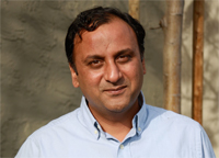
Sandeep is currently a consultant at Mskribe. Most recently he was Vice President of West Coast Operations, for CLK-Design Automation. Prior to CLK-DA, he was CEO and Founder of Synchronous-DA which merged with CLK-DA and a history going back through Cadence and HLD Systems. He began is career as a CAD engineer at AMD in the x86 group.

EDA and the 50 picosecond problem

There has been a lot of introspection and analysis recently, by EDA executives and analysts as to why we are where we are, as an industry.    There seem to be no easy answers as to why EDA is at the bottom of the economic food chain, in-spite of the stellar growth and demand for electronic devices. We can blame the recent economic crisis, declining ASIC design starts, rising mask costs etc. but the writing was on the wall much before the market meltdown.

EDA ecosystem revisited

One can point to many issues with the EDA industry, and attempt to root cause why we are not being able to get a bigger piece of the semiconductor pie. Few things that come to mind are the following:

The venture capital community seems to look at EDA as a broken business model, with little or no upside, due to the lack of recent exits. An investor recently told me and I quote “The smallest ROI per Phd. is in the EDA industry”.

Large EDA vendors are not feeding the ecosystem.There has been little or no funding for startups or academic research from the large EDA vendors. In addition there is less and less collaboration from the large EDA vendors.While this approach is conceivably good to protect ones’ franchise, it maybe a flawed strategy for the long term, in a technology driven industry such as ours.

Funding for research institutions has fallen out of favor with EDA companies.This is a disturbing trend, considering the fact that a majority of the foundation of EDA software comes from university research.

Large EDA vendors want to mimic the enterprise software (Oracle, SAP) monolithic model. This sounds very attractive to a CEO of an enterprise, as compared to a heterogeneous ‘best-in- class’ model, which would entail internal support and development.The one difference in EDA versus enterprise software, is perhaps the fact that FASB (Financial Accounting Standards Board) or GAAP (Generally Accepted Accounting Principles) rules don’t change at the rate at which the semiconductor process or design requirements change.

EDA startups have always relied on Angel investors who were as passionate about EDA technology as the founders.This is another very important source of capital that is drying up, and is perhaps the one that has serious implications for us as a technology industry. If successful EDA “Angels” don’t feel comfortable investing in our industry, this say’s that we have a serious problem on our hands.

Semiconductor industry (our customer base) has been slow to adopt new technologies, due to cost pressures. In addition they have got used to getting products for a fraction of what they used to spend 5 years ago.This trend compounded by a lack of pricing discipline from the EDA vendors has lead to significant price and value erosion.EDA industry’s disaggregated software ecosystem is clearly hurting the industry. If companies differentiate themselves based on a file format ( CPF versus UPF for instance) , we have some critical thinking to do, as an industry. Efforts such as Open-Access have not gained the traction they should have to propel our industry from competing on issues that add little or no value, such as proprietary file formats. Perhaps ‘Open-Access’ needs to be more ‘open’.

The 50 picosecond problem

The final problem that comes to mind is what can be termed as the ‘50-picosecond problem’. This is a problem where innovation seems to stall when an industry segment nears maturity.

In order to highlight the ’50 picosecond problem’ we can try to analyze the IC physical design tool segment of the EDA industry, as an example.

IC physical design tools from Company S, Company C , Company M and Company M can take the same design and produce results within 50 picoseconds (figure of speech rather than a literal) of each other.

What this highlights is a lack of differentiation amongst physical design tools. In addition, we see new startups in the physical design space, that develop a tool from ground up, only to be marginally better (50 picoseconds ?) than the incumbent tools.

What could be reason for such incremental differentiation in products that are developed from ground up, with the premise of displacing incumbent tools ? Perhaps all the engineers are reading the same books, and implementing the same algorithms again and again ? Could it be that the semiconductor process is scaling so well, that there are no new disruptive physical effects ?

No easy answers

We will attempt to address some of the issues highlighted above in a later blog entry.

Posted in guest blog | Comments Off

The VHDL and Verilog story

I put a blog entry up on the Oasys blog about their new release, which is the first to support VHDL. But a couple of people told me it was a nice recounting of history so I decided to put a more generic version over here.

VHDL is, of course, one of the two main hardware description languages dating back to the 1980s. The history of Verilog and VHDL is quite interesting. Verilog was originally created by Gateway Design Automation. Gateway was subsequently acquired by Cadence for what seemed like a very high valuation at the time, although of course it has probably been one of the most successful acquisitions Cadence did when you think of the sales of Verilog that they have made over the intervening years. VHDL, which is actually one of those nested acronyms since it stood for VHSIC Hardware Description Language, with VHSIC further parsed down into Very High Speed Integrated Circuit. The VHSIC program was run by the US DoD and VHDL looked for a time that it might become the dominant standard, since Verilog was a proprietary language owned by Cadence.

But Cadence opened Verilog up and let other people participate in driving the language standard. As Gordon Bell once said, the only justification for VHDL was to force Cadence to put Verilog into the public domain. But having two languages has been a major cost to the EDA industry for very little gain. VHDL was a very powerful language but in many ways was less practical than Verilog. For instance, you could define your own values for any signal. But that meant that gates from one library wouldn’t necessarily interact properly with gates from another library (sounds like some of the problems with TLM models in SystemC that are finally being resolved). So that required a new standard, VITAL, so that gate-level signals were standardized. The richness of VHDL abstractions meant that it was and is used for some of the most complex communication chips. Model Technology (now part of Mentor) had probably the best VHDL simulator that they sold cheaply, and that helped to make VHDL more standard in the FPGA market than Verilog. Despite the fact  that a Verilog simulator is easier to write than a VHDL simulator, it sold for a higher price for years. This has led to an odd phenomenon where some of the most advanced chips are done in VHDL, and many of the simpler ones.

Anyway, the dual language environment (and, of course, SystemVerilog has arrived to make a third) continues to exist. Almost all tools have, over the years, bitten the bullet and provided dual language support for both VHDL and Verilog. Often the front end for VHDL, which is a complex language to parse, comes from Verific (as does the VHDL front-end for Oasys’s RealTime Designer).

Posted in eda industry, engineering | Comments Off

Guest blog: John McGehee

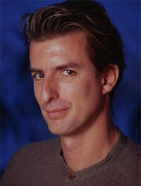
Today’s guest blog is by John McGehee. John is a independent consultant in Silicon Valley, specializing in EDA application development, design methodology and Japan.  He blogs about these topics at www.voom.net.  Prior to starting his consulting career, John was an AE at Avanti, Cadence Japan and Daisy Systems Japan.

How I got to Japan

The PA system at work announced that I had a call. It was from Dr. Steve Butner, my graduate advisor at UC Santa Barbara. He was very excited. “John, I just got some information about this program that was just made for you.” He explained that the American Electronics Association was sending electrical engineering and computer science graduate students to an intensive Japanese language course, and then on to work as an engineer in Japan. The goal of the program was to balance the exchange of engineering students between Japan and the US.

I had already taken two years of Japanese classes. I dreamed of applying the language at work in Japan, but I had no way to actually make this happen. The American Electronics Association Japan Research Fellowship was the opportunity of a lifetime to realize my goal. I applied, and was accepted. Had the program never found me, my dream would have just quietly faded away.

The fellowship was a full ride: airfare, room and board, tuition at Cornell, and a job as a chip designer at Intel Japan. All of this was a tremendous gift for which I am eternally grateful. Only the power of a major industry association could make something like this happen.

I too was going to pay. This episode of my life was like a card game in which I held a great hand, but nonetheless discarded graduate school, my girlfriend, job, friends and Santa Barbara, retaining only my electronic engineering card. Then I was dealt new cards I could not even recognize. How would I assemble them into a winning hand?

The program started with the Cornell University FALCON Japanese language summer session. This was superb. I was very serious and studied hard. When I started, I had an understanding of Japanese grammar, writing and vocabulary, but I could not really hold a conversation. Just nine weeks later, I could carry on relationships with people entirely in Japanese. I have never learned so much so quickly.

I vividly remember seeing Japan for the first time from the air. All this preparation, and I had never even been there. I hired a taxi and chatted with the driver in Japanese along the way to my destination. Using a new language in country for the first time is the most exhilarating of experiences.

I arrived in Tsukuba, where a tiny apartment awaited me. It had a murphy bed, a basic kitchen, a bathroom and a television, which was to be my language teacher and only friend for quite a while. My private apartment was a palace compared to the barracks provided to the other AEA Japan Research Fellowship participants. Intel even gave me a new Toyota Corona to drive.

My job at Intel Japan was verification and circuit simulation for the 8253 counter/timer portion of a microprocessor. As you might expect, many signals described a count. Engineers and programmers usually abbreviate this common word as “cnt”, but the Japanese designer chose to delete only the “o” in “count”. It made for the most profane RTL and netlist I have ever seen.

Intel Japan is based in Tsukuba, a “Silicon Valley” created artificially by the government. These are the same people who brought you Narita Airport, located an hour away from the city it serves. Tsukuba is in Ibaragi-ken, which is famous for backwardness. The nearest train station was 30 minutes away by car. In Japan, a city without a train station is nowhere. I hated living there, and so did many others. All the foreigners at Intel Japan were plotting their escape to Tokyo. Some Tsukuba residents escaped in a more tragic way. The suicide rate was so high that Tsukuba had its own trademark method of suicide–Tsukuba diving, throwing oneself off Tsukuba Tower.

Instead, I threw myself into improving my language skills, the goal for which I had sacrificed so much. This meant using exclusively Japanese. It also meant extreme isolation, as I was not a particularly engaging conversationalist. Still, I was good enough to carry out my duties at Intel in Japanese, speaking English only to my boss (a wise compromise). In an EE Times interview I declared, “I’m known as hardcore about not speaking English in the office. I am definitely looking at getting very good at Japanese.” Ah, such youthful bravado. Hardcore indeed.

My colleagues at Intel were more sophisticated than the locals, and they were kind to me. In the winter, we went skiing almost every weekend. I made some good friends at Intel Japan. After about six months, the loneliness and culture shock started to subside.

Originally my internship was six months, but I was just starting to get the hang of things, so I extended to one year. Intel Japan was good to me, but they only had engineering work in Tsukuba. As the end of my year came to a close, I conducted a job search, and landed a position in Tokyo. After a few years, I returned to finish graduate school at UCSB, then set out for Japan again. The AEA Japan Research Fellowship had succeeded in its goal of turning me into an engineer who could navigate Japan.

Posted in guest blog | Comments Off

NXP, cochlear implants, LED lighting and more

A couple of weeks ago I spent a morning at NXP’s innovation day. The first slightly surreal aspect of it was that it was in a building I used to work in. After I left VLSI Technology, NXP (then Philips Semiconductors, don’t forget that final “s”) made a successful bid for VLSI and then consolidated their operations in silicon valley into the 4 buildings that VLSI had purchased when its landlord had gone bankrupt. After several rounds of layoffs there are apparently just 250 people working in buildings that I would guess could accommodate 10 times that many people.

Since NXP was spun out of Philips they have divested themselves of their wireless business (sold to ST and now consolidated into ST-Ericsson) and their low end analog business (to Virage). They are also spinning out their digital TV and set-top-box and combining it with Trident. This means that the remaining part of the business can focus on high performance mixed-signal designs, especially ones requiring non-standard manufacturing processes that you can’t just order up from the foundries.

If you want some numbers, NXP grew 20% in Q3 from last year to just over $1B (which I must say is not bad in the current economic climate). They made $147M on that. They also have just over $1B in cash, which apparently is more than all but a handful of other semiconductor companies (although, of course, many semiconductor companies are integrated into larger electronics companies, especially in Asia).

By high performance mixed signal NXP means a combination of SoC technology, riding Moore’s law in the usual way, and mixed in with high-performance analog, sensors, special packages, high-voltage, RF, biological interfaces. In many of the submarkets of this NXP is already #1 and, with mixed signal expertise being scarce, likely to stay that way.

The most interesting of the products that they demoed was a cochlear implant where the left and right ears implants could communicate with each other using very short range wireless technology. Cochlear implants are put inside deaf people’s skulls to interface directly to nerves. Gradually the deaf person (usually a child) can start to hear as the brain works out what to do with those weird electrical signals that suddenly started to appear. I have a friend whose daughter was born deaf and has a cochlear implant and the transformation is nothing short of incredible. But putting two implants, one for each ear, and having them be able to communicate with each other, makes for even better comprehension. With an inductive interface too, it is possible to use a small box that takes Bluetooth and communicates inductively with the implants, allowing deaf people to use the phone or listen to music much more easily (it’s too power hungry just to put a bluetooth receiver in the implant, remember it’s hard to change the battery).

Another interesting technology is LED lighting. This is not ready to show up in yor home yet, but it is ready for street lights and close to being ready for commercial applications, where a bulb burning out is not just an annoyance but an expense. Although they use less power, and so save money there, the real saving comes from the fact that they last so much longer.

Posted in semiconductor | Comments Off