 This is the first of several posts about 3D ICs. I attended the 3D architectures for semiconductor integration and packaging conference just before Christmas. I learned a lot but I should preface any remarks with the disclaimer that I’m not an expert on the subject, but I now know enough to be dangerous. But most people are not experts on this subject so I think it is worth a high level overview of what is happening.
The first thing is the 3D chips do seem to be happening. There are designs in production, there are lots of pilot projects and the ecosystem (in particular, who does what) seems to be starting to fall into place.
The first approach to talk about is flipping one chip and attaching it to the top of another. This is done by creating bonding areas on each chip, growing (usually copper) microbumps to create die-die interconnect at a pitch of approximately 50um. The big user of this technology is in digital camera chips. The CCD image sensor is actually thinned to the point that it is transparent to light and then attached to the image processing chip. The light from the camera lens passes through the silicon to the CCD unobstructed by interconnect etc which is all on the other side of the sensor.
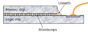
 This approach is also used for putting a flipped memory chip onto a logic chip (see picture). It is not well-known, but the Apple A4 chip is built like this, with memory on top of the processor/logic chip. There are now standardization committees working on the pattern of microbumps to use for DRAMs (analagous to standard pinout for DRAMs) so that DRAM from different manufacturers should be interchangeable. Unlike in the picture, the bumps are all towards the center of the die so that the pattern is unaffected by the actual die size which may differ between manufacturers and between different generations of design.
Although this technology is formally 3D, since there are two chips, it doesn’t require any connections through any chips and is a sort of degenerate case.
You probably have heard that the key technology for real 3D chips is the through-silicon-via (TSV). This is a via that goes from the front side of the wafer (typically connecting to one of the lower metal layers) through the wafer and out the back. The TSV is typically about 5-10um across and goes about 8-10 times its width in depth, so 50-100um. A hole is formed into the wafer, lined with an insulator and then filled with copper. Finally the wafer is thinned to expose the backside. Note that this means that the wafer itself ends up 50-100um thick. Silicon is brittle so one of the challenges is handling wafers this thin both in the fab and when they have to be shipped to an assembly house. They need to be glued to some more robust substrate (glass or silicon) and eventually separated again during assembly. The wafer is thinned using CMP (chemical mechanical polishing, similar to how planarization is done between metal layers in a normal semiconductor process) until the TSVs are almost exposed. More silicon is then etched away to reveal the TSVs themselves.
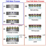
 The picture to the right (click for a bigger image) shows Samsung’s approach. FEOL (which, for you designers, means front-end of line which means transistors and is nothing to do with front-end design) is done first. So the transistors are all created. Then the TSVs are formed. Then BEOL (which means back-end of line which means interconnect and is nothing to do with back-end design). After the interconnect is done then the microbumps are created. The wafer is glued to a glass carrier. The back is then ground down, a passivation layer is applied, this is etched to expose the TSVs and then micropads are created. This approach is known as TSVmiddle since the TSVs are formed between transistors and interconnect. There is also TSVfirst (build them before the transistors) and TSVlast (do them last and drill them through all the interconnect as well as the substrate).
There are two design issues with TSVs. First is the exclusion area around them. The via comes up through the active area and usually through some of the metal layers. Due to the details of manufacturing, quite a large area must be left around the TSV so that it can be manufactured without damaging the layers already deposited. The second problem is that the manufacturing process stresses the silicon substrate in a way that can alter the threshold values of transistors anywhere nearby, thus altering the performance of the chip in somewhat unpredictable ways.
