Guest blog: John Lambert

Today’s guest is John Lambert. He is another Brit and is currently CEO of Virtutech (I was his VP marketing for a time). Prior to that he still has the scars from many years at Rational starting from the early days up until IBM acquired them, originally back in the UK and then over here. His blog was due to go out earlier but he has the modern equivalent of “the dog ate my homework."

His entry echoes some of the things that came up at last week’s DVcon panel, that IC design is only a part of the design problem.

Near death experiences

When, a few weeks ago, Paul asked me to write a blog entry, essentially to cover his rear end whilst he was gallivanting about in Mexico, I duly sat down and began to pen something suitably earnest on the future direction of EDA. Then, while twiddling my thumbs and staring out of the window hoping for some lightning bolt of inspiration to strike, I read a few of the earlier posts in order to get some more context. Fast concluding that in fact I had little new to say in that regard, I thought I’d do something different and instead focus more on the bigger picture. I’d construct a grand, sweeping, vision of how product development would look in the 22nd century and what collectively we’d all need to do in order to get there.

It was all going swimmingly well until one Thursday night when my laptop tried to commit suicide by downloading a poisonous .Net update all by itself. Not sure why. Perhaps the whole futility of it all triggered some innate nihilistic tendencies buried deep within Windows Vista – because Lord knows they are in there somewhere, as any regular user of that abomination will readily testify – but whatever the reason, the net result (pun intended) was that by the time the PC was suitably detoxified I’d lost the thread of the epic story I was going to tell. Here instead, therefore, are a few basic points that I will make in the form of blank statements without bothering to justify any of my thinking. It’s just easier that way.

  1. Follow the money. OEMs are in the business of building and selling things. Those things include chips and software, but that’s entirely incidental to the business they are actually in. The things they sell are either few in number and very expensive, or manifold and cheap, but either way those guys are the ones coining it, not the purveyors of the necessary picks and shovels. No use whining about it, that’s just the way life goes.
  2. Complexity kills. Making stuff is hard, and getting harder. Everybody wants the things they buy to do more, be cheaper to buy, breakdown less and to be available sooner. Year-by-year, this makes the whole shooting match harder to manage regardless of volume, price or scale.
  3. It’s good to talk. Building stuff has become multidisciplinary. Alas, we got here through rigid specialization. Stovepipes are good at keeping stuff contained, managed and concentrated (smoke, most typically) whereas what’s now most important are things like collaboration, iteration and exchange. This is a fundamental industry shift that is still only in its infancy. It’s important, OK?
  4. Don’t sweat the small stuff. Why spend another $5m on upgrading your ASIC design tools when the end product, an ASIC presumably, accounts for only 20% of the hardware, the design and development of which consumes just 10% of the overall project budget? It makes no sense. Ditto buying a better compiler or smarter test tool. “Commoditization is murder”. Now there’s a slogan to live by. Or do I mean die by?
  5. Complacency is death. So why on earth are all the EDA companies seemingly so stuck in their own stovepipe, refusing to strike out and fully embrace the broader product lifecycle? At least, that’s what you’d conclude from a number of the posts here, and indeed from looking at how intent they seem to have been over the past few years on getting better and better at serving the needs of a market slice that’s been getting smaller and smaller. Just how bad does the economic outlook for the industry have to be before one of the herd strikes out on their own to find greener grass way over yonder?

Someone, somewhere, soon will figure out that there’s room for one company to do for product America what the likes of IBM, HP and others have done for enterprise America, namely, to become the one partner that can pull together the deeply divided worlds of EDA, PLM and software, forging in the process a vendor with the breadth to truly breakdown those silos, thereby paving the way for the creation of new and innovative development processes. This HAL Corporation will supply both tools and techniques – process as well as product – that allow customers to systematically and repeatably shorten the overall end-to-end cost of designing, developing and delivering a new product. As a result, hundreds of man years of effort will be shaved from the total development bill, delivering results in timescales dramatically shorter than anything possible today.

All of this will happen because it has to happen. Market forces demand it, complexity dictates it. It just requires someone with the cojones to strike out, to make the first and boldest of moves.

Anyone want to lay bets on the most likely candidate to lead that charge?

Bottom-line: it’s time to welcome in the revolution; further polishing of the current stovepipes only results in shiner stoves, not warmer houses. I rest my case.

Posted in guest blog | Comments Off

Fab 5

For some time I have been talking about the semiconductor industry as the Fab 5, since there have been five process “clubs”. A few players hedge their bets and are in more than one club. The fab five are Intel (a club on its own), UMC (along with Xilinx and Texas Instruments), IBM (along with Samsung, ST, Infineon, AMD, Sony, Freescale and Chartered), Japan Inc (Renasas, Toshiba, Fujitsu, OKI, Sharp, Sanyo, Matsushita) and the big one TSMC (with AMD, TI, NXP, ST, LSI, Sony, Qualcomm). Japan Inc in particular is messy with Toshiba tied closely to NEC (in the TSMC club) but to Sony (in the IBM club too), Renasas and Fujitsu are still sort of going it alone. Japanese politics would indicate that they will all get together somehow.

Big changes are afoot. Here are some of the things going on, ST, NXP and Ericsson wireless are all merged together into a new company (called, yawn, ST-Ericsson). Nokia has also sold its wireless unit to ST so it is presumably in there somewhere. Toshiba looks like it is going to really join Japan Inc (as if there was any doubt). TI and Freescale are both trying to find a home for their wireless groups but nobody wants them at a price they want to sell. The IBM club have deepened their technology agreements and ARM (although fabless) seems to be sort of joining the IBM club to help create energy-efficient SoCs, with Samsung both building and consuming the volume (and so I hereby rename the IBM club the Samsung club).

What about everyone else? AMD, ATI (also in AMD for now), MIPS, nVidia, UMC, NXP, Infineon, Motorola, Texas Instruments, Freescale were all bleeding cash even before the downturn got really bad, and they are reducing their footprints. All of Japan Inc except maybe Toshiba were also bleeding money (and Toshiba would have been except for all that flash going into phones and iPods, and is now hurting more after losing Xilinx to Samsung over price).

So based simply on financial strength it looks like the 3 fabs are going to be TSMC, Intel and Samsung (taking over the name badge for the IBM club) long-term. Of course other people like ST won’t lose their fabs overnight but they won’t be able to afford to keep up. And it is unclear how many of the memory houses will make it through the current downturn. Qimonda is clearly comatose already and isn’t going to wake up.

So the Fab 5 will become the Fab 3. For EDA this just emphasizes that there are too many EDA companies, as I’ve said before. Or maybe that EDA will go internal again, which is a discussion for another day.

Who would have predicted 20 years ago when TSMC was a small foundry with a non-competitive Philips process that it would be the dominant player. Kind of like predicting that Ringo would be the last Beatle of the Fab 4…oh wait, maybe that’s going to happen too.

Posted in semiconductor | Comments Off

No sex before marriage in EDA

Temple
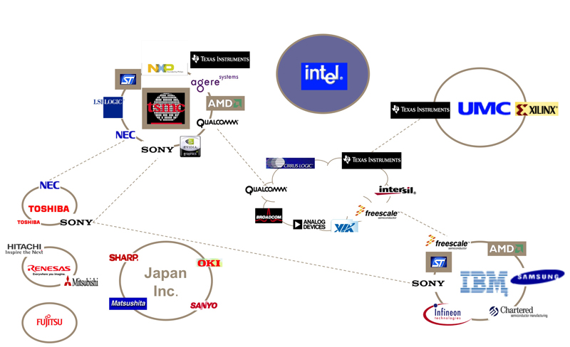
In most businesses, every company doesn’t feel the need to make every product that it sells. When you buy a car from General Motors, they don’t make the ABS system themselves, they buy it from Delphi or from Bosch. When DEC came out with the Vax, they didn’t feel the need to make their own graphics terminals, they bought them from Tektronix and re-badged them.

This is known as an OEM deal. OEM stands for “original equipment manufacturer” and refers to the fact that General Motors is the manufacturer of the original equipment (the car) and the other parts are treated by regulation as if GM had made them themselves. Indeed, they may even badge the part with their own logo and make it hard to find out just who is the real manufacturer.

OEM in other industries has come simply to mean re-selling stuff created by another company. In EDA software, for example, almost everyone’s schematic viewer is actually a product from Concept Engineering in Germany.

But this sort of deal, where a component of the product is incorporated from an external company, seems to be the only sort of OEM deal that works. Once the deal moves up to the level of a whole tool then OEM deals almost never work in EDA. There seem to be two reasons for this, one on the customer side and one on the vendor side.

On the customer side, if you are buying a product from bigEDA and you know that it really comes from littleEDA, then why would you not want to deal with littleEDA directly? If you have a problem, you know that bigEDA is just going to pass the question onto littleEDA anyway, and even before you buy it there may be some channel conflict when both bigEDA and littleEDA are competing for your business, and for sure the littleEDA sales team knows much more about the product. It just doesn’t make too much sense to flow your dollars to littleEDA through bigEDA, and flow their support back through the bigEDA support channel.

On the vendor side, bigEDA wants to do big deals with their major customers. They’ll give you all your EDA software, or a good part of it, for all your EDA budget, or a good part of it. OEM deals usually require a per license payment from bigEDA to littleEDA but that doesn’t fit well with a deal where technically the semiconductor company may be getting unlimited or a large number of licenses for a bundled sum. There is simply no way to calculate an appropriate number of license fees to pay littleEDA, and the need to do so makes the deal more complex and so the salesperson simply drops the OEM product as not worth the usually minimal increment in bookings.

Finally, there is a strategic reason that makes OEM deals unattractive. You’d think that an OEM deal would be sex before marriage. If the deal works well then bigEDA can buy smallEDA. The trouble is, if the deal works well then another big EDA company might make a move. And either way, bigEDA is going to have pushed up the price of smallEDA and is going to have to buy back their own revenue. There’s no sex before marriage in EDA. If smallEDA is the right company then marry them immediately before they get more expensive.

Posted in eda industry, marketing | Comments Off

We’re driving in a fog

I went along to what used to be John Cooley’s EDA bigwigs panel and is now Peggy Aycinena’s “Is EDA dead or alive?” I had to keep asking myself am I dead or alive for the first part of the panel as each panelist insisted that their company was not suffering at all in the current downturn, there were no layoffs, and every EDA engineer gets a pony for their daughter. I may have misheard that last bit.

Peggy set the tone in her opening by stating that EDA tools are too cheap. I’ve pointed out before that there isn’t enough money flowing into EDA overall, and that it is pathetic that EDA only gets $4B out of the multi-trillion dollar electronics market. But that is different from claiming that everyone is getting tools too cheap.

Of course EDA, in the sense of software, has to continue to exist, as Ajoy Bose of Attrenta pointed out. But it is a fallacy to assume that this means that the EDA industry will continue to exist as currently structured.

Ravi Subranamian of Berkeley Design Automation described his customers as “driving in a fog” and they don’t know how long the fog will last so they are driving very carefully, in particular focusing on cost.

Diana Raggett of Javelin had just been to Taiwan. Customers are all on 4 day work-weeks going down to 3. In Hsinchu science park, three-quarters of the companies are on 1 day work-weeks. Of the 300 fabless companies in Taiwan and 500 or so in mainland China, less than half are expected to survive.

Gary Meyers of Synopsys has the evidence of quarterly results beating expectations. Echoing something I’ve heard Aart say, he related how high level management at customers is rethinking their future and willing to engage in different kinds of relationships. He continued to point out that Princeton has more people in their financial engineering program than electronic engineering program. That problem is obviously self-correcting, but I doubt that electrical engineering is necessarily going to be the beneficiary.

Scott Sandler of Springsoft amitted that customers are struggling and revenues are lower than expected. We were all shocked, shocked to hear it.

Tom Sandoval of Calypto fell on his sword too, admitting that their verification business was constrained but the power-redution business was also benefitting from people wanting low power chips right now.

Peggy pointed out that semiconductor companies are doing more internal development, and that if she was running a semiconductor company she’d want to do all internal development to keep control and to have algorithms optimized for her process. Since her process is almost certainly TSMC (unless she gets Paul Otellini’s job or the CEO of Samsung) then that is the same process as everyone else. There is not much integrated about an IDM these days. The panelists didn’t feel this was any sort of threat or was likely to make any change in the industry structure.

Peggy’s latest column was about using EDA algorithms in biochemistry, nanotechnology and other areas. But she couldn’t get anyone on the panel to really look at this as being a way to enlarge Joe Costello’s bowl of dogfood.

Suddenly the focus shifted to whether EDA was getting any of that bailout money. Did EDAC even communicate with Washington? I’ll be the first to admit that most of the money in the stimulus bill is going to be wasted, but when EDA is lining up behind GM and Chrysler I think we are looking in the wrong place.

Gabe Moretti (in a question that wasn’t a question from the audience) pointed out that EDA really is small at $4B, that electronics is only one part of design and maybe someone should look at the big picture. But it was too near the end and so nobody took the bait, we all went downstairs for a glass of free wine instead.

I think Peggy’s question about internal development, and Gabe’s about tackling the bigger picture are really key questions. Meanwhile the convention of buggy whip and related operators are focused on better and better leather and fighting for market share among their aristocratic customers.

Posted in eda industry | Comments Off

Guest blog: Grant Martin

TGrant Martinoday’s guest blog is from Grant Martin, Chief scientist at Tensilica. He worked for Burroughs in Scotland (in Cumbernauld, of all places, which makes Newark look attractive), Nortel in Canada, and then at Cadence before moving to Tensilica. He literally wrote the book on system design, most recently co-author of “ESL and System Design”. The British press used to have a rule that they would never mention another newspaper by name, but just say something like “in another newspaper.” Well, Grant has his own blog in another newspaper.

In some ways this a continuation of the power theme. Remember that it is much more power-effective to run a small processor at just the right slowish clock rate, than it is to run a powerful processor at huge clock rate for a short time and then idle it or shut it down while the rest of the system catches up.

Processor v hardware: the winner is…

 “Everyone” knows that processors are more flexible because they’re programmable, but “everyone” knows they are slower than dedicated hardware for high-performance algorithms.   But how do you decide between processor and hardware? There is a third way that lies between.

Although I do my best to ensure that designers I meet understand the idea of an   application-specific instruction set processor (ASIP), many people have never heard of them.   If they have, they may not realise that designers can configure them with automated tools.     And an ASIP is often so close to the performance, power consumption and area of dedicated hardware, that it is a superior option – especially with programmable flexibility.

Everyone is familiar with fixed general purpose processors, used for control tasks.   And fixed digital signal processors (DSPs) are found in many devices for data-intensive tasks – the ‘dataplane’. But what many don’t realise is how powerful the combination of configurable, extensible ASIP technology and dataplane tasks can be, compared to either a fixed processor or dedicated hardware.

Audio processing is an excellent example. An ASIP customised for audio, together with the right codec software, can decode MP3 running with a clockrate of just 5.7 MHz, producing near-CD quality sound and dissipating only 0.45 mW in TSMC’s 65nm LP process (details). Because this is a processor, other audio codecs can be downloaded to an audio player in the field long after it is sold.   Dedicated hardware could never provide this level of flexibility, and may not offer any significant advantage in performance, power or cost. Achieving 100+ hours of battery life on a portable audio appliance is more than possible with ASIPs.

Video is another dataplane application that can be mapped to ASIPs.   Standard definition decoding can be accomplished on a multiprocessor video subsystem running at 200 MHz in a TSMC 130 nm G process (details). And there are many other products, from baseband in wireless communications to high performance network processing, where you will find ASIPs.

ASIPs change the way in which system architecture is conceived. “Classical” hardware designers have a bias to implementing everything they can in dedicated hardware. “Classical” software developers have a bias to implementing all functions on general purpose processors – and running them at very high rates if necessary.   Running audio on a control processor at hundreds of MHz is possible, but hardly optimal. An ASIP-aware architect will instead use different tradeoffs. 

They will start by mapping control tasks to one or a cluster of control processors – in the latter case, possibly a cache-coherent “multicore” where processors can be powered down when not needed.   But every dataplane task is an opportunity to use ASIP technology.   Dedicated hardware blocks become a last resort – used by necessity, in order to meet system performance or energy consumption goals.   The result is a heterogeneous ASIP-dominated multiprocessor design where subsystems can be powered down whenever possible to minimise energy consumption.

Some recoil at the idea of sprinkling many processors in a design and “wasting” them when not needed. I remember the keypunch/card-reader/line-printer “cafeteria” line-up feeding the University of Waterloo’s mainframe. In that era, every computer cycle was indeed too precious to waste. 

But times change and the concerns of our youth give way to modern needs.   These days, every joule of energy is too precious to waste. Using ASIPs brings energy-efficient computation and communication to the exact places where they are needed. So the winner of “processor vs. hardware” is “neither” – but rather, the ASIP that lies in between.

Posted in guest blog | Comments Off

Power again

Power outletYesterday I promised an overview of what power reduction techniques are out there. First, a disclosure: I was interim CEO of Envis for about a year and I’ve done some consulting for Nanochronous.

Firstly, there are two kinds of power: dynamic and static. Dynamic power is used in switching signals inside the circuit. It is affected by operating frequency and voltage. Static power is dissipated whether the circuit is doing anything or not, and mostly is leakage power through transistors that are supposedly off but in fact leak a little current. This was not a problem above 100nm or so, but below transistors are not so much on and off, as bright and dim.

The most common way to control leakage is to use special libraries that have two versions of each gate (or most gates). One is slow but has low leakage. One is fast but leaks since it never truly turns completely off. On the critical path the fast leaky gates are used; off the critical path the non-leaky slow gates are used. Synthesis tools will choose the cells automatically based on the timing constraints.

Taking this technique a little further was Blaze DFM whose tool would make tiny adjustments to the mask data for transistors off the critical path, lowering their performance but making them leak a lot less. TSMC licensed this technology and Tela announced yesterday that it was acquiring them.

The most common dynamic technique is clock gating. The old rules used to be to do purely synchronous design, and clock every flop on every clock cycle. If a register was only loaded with a new value sometimes, then a multiplexor was added to recirculate the old value back to the input so that when the flop was clocked it would re-latch the same value as it was already holding. The simplest form of clock gating is to replace those multiplexors with a clock gating element (CGE) that inhibits clocking the flop when the value doesn’t change. This doesn’t win you anything on a single flop, but if it is, for example, a 32-bit register then 32 muxes can be replaced with a single CGE saving on area, and, because the effective clock rate of the register is reduced, power. By clever circuit analysis it is possible to find more complex circumstances under which registers can be suppressed either combinationally (the value really wasn’t going to change) or sequentially (the value might bave been going to change but no output from the circuit would noticed the change). All the synthesis tools, most notably Synopsys Power Compiler, do the mux replacement. Calypto and Envis are two companies automating the more extensive gating approaches.

Next there is a whole spectrum of techniques that depend on voltage islands. A voltage island is an area of the chip with its own power supply. Obviously this has a major impact on physical design since the island must correspond to a particular region of the die. The first thing that can be done with voltage islands is simply to power them with different supply voltages. Those on a lower voltage will have lower performance, of course, but they will also consume lower power, both static and dynamic.

Power down is another common technique. Voltage islands which are not being used are turned off completely by turning off their power supply. When you are not making a call on your cell-phone, the gates used to process transmit and receive data are not required and can be turned off. This needs to be done carefully, or else the current inrush when the island is turned back on can cause the voltage to drop elsewhere on the chip. Typically this means that the island must be powered up slowly using small transistors and then finally brought up to operational level by turning on much larger transistors. Powering down blocks is always done under software control but the powered down block needs to be isolated from the rest of the circuit so that its output signals do not drift and cause crowbar current and waste power elsewhere. There are no tools for automatically finding areas to power down. The software not the netlist would be the place to look. The CPF and UPF formats have extensive support for power down.

As we get deeper below 100nm, the variability of processes gets much wider. This means that the typical chip and the worst case chip are getting further and further apart and so the penalty of designing to worst case design, given that most chips are typical by definition, gets larger and larger. Adaptive voltage scaling is a way to handle this. Use on-chip circuitry to measure the actual performance, and then lower the voltage (saving both dynamic and static power) just the right amount that the chip still runs at the correct speed.

One adaptive solution involving off-chip voltage regulators is National Powerwise. They have put this in the public domain since they make their money selling the off-chip voltage regulators. Nanochronous builds copies of critical paths and uses these to adapt the clocking to the environment (process corner, voltage, temperature) so that the chip will automatically consume less power but still run to spec as the voltage is lowered. Elastix does something similar, adapting the performance of the chip as the voltage is altered, while taking the process corner into account. Handshake removes the clock completely and runs asynchronously with whatever performance is appropriate given the power supply voltage. Nanochronous is in Greece, Elastix is in Spain, and Handshake is in Netherlands; it must be something in the wine.

The next approach is to vary the voltage to islands while the chip is being used, rather than having fixed, but different, power supply voltages for each island. When the voltage is changed under software control it is known as dynamic voltage and frequency scaling. This is a technique that is talked about a lot and used only a little, as far as I can tell. The idea is that if your microprocessor (or whatever) is not doing anything very important, why not run it slowly. And when it is in heavy computation mode run it flat out. To do this is tricky though. To slow it down the frequency must be lowered, and then (and only then) the voltage can be lowered. To speed up, the voltage must be raised, which takes time if it is not going to create a lot of power-supply noise, and then the frequency can be bumped up.

A lot of power gets consumed in the clock tree itself. Certainly 30% and sometimes 50% of the total power. Azuro works on laying this out and placing the gates more sensibly than is typically done by the clock tree synthesis built into every place and route tool.

Cyclos has another approach to reducing the 30% consumed in the clock. They think that clocks are the wrong shape, being square waves. If the clock was a sine wave then it could be resonant if we added some inductors, and would not consume power in the clock tree. That would be nice but the price is that every clocked element needs to be adapted so it can work with a sinusoidal clock rather than the usual rising-edge, falling-edge square wave we are all used to.

No list of all companies in the power area would be complete without Sequence, some of whose ancestral companies have been around for over 15 years. Their primary focus is on measuring power, with or without vectors, at netlist or RTL level. They are pretty much the standard tool for this.

There may be other c
ompanies out there focused on power reduction. As I said yesterday, “power is the new timing” and so it is a focus of a lot of innovation.

Posted in methodology | Comments Off

Blazing a trail

The mystery of whether Blaze DFM had closed down or not is over. It has been acquired by Tela Innovations mainly, it would seem, for the PowerTrim technology that had been licensed by TSMC. A major strategic relationship between Tela and TSMC was also announced. Both these are interesting developments..

Tela acquiring Blaze is interesting primarily because neither company is public: one private company is acquiring another (Tela is not venture-backed but funded privately, which is a story for another time).  I think that this is something that we will see more of in future, especially in the year ahead, along with other acquisitions as small companies run low on cash and need to find partners. Historically small EDA and semiconductor companies would either get large enough to go public or be acquired by the larger healthy companies in their industry. Obviously for the time being and perhaps for a long time the public markets are closed, and the larger companies are not really healthy enough to be making any major acquisitions (despite Synopsys’s better than expectation results) nor do they have the cash to pay up. And nobody is borrowing anything anytime soon (with the federal government wanting to borrow a trillion dollars why would people with cash lend to anyone else).

The other interesting aspect of this is TSMC partnering with Tela over not just Blaze’s technology but their own. The basis of this technology was described in a guest blog last week by Mike Smayling. This was coincidental since I didn’t know about this announcement then. It just seemed a good time to talk about lithography since this week it is SPIE, the big conference in lithography. And remember, Moore’s law is largely about driving lithography and its ecosystem forward.

TSMC will likely be using Tela’s technology to create value added options for their foundry users, They had previously done this with the Blaze technology, supplying it as a premium service  with a wafer royalty. Now, although I don’t know the financial details of the details, presumably doing the same with Tela but on a much larger scale. Tela’s technology is much more widely applicable and the alternatives are much more limited, especially at the nodes below 45nm where current OPC techniques run out of steam and some form of restricted design rules becomes essential. You simply can’t print arbitrary layout any more.

Going back to beginning, and whether private companies or public companies, are the most likely eventual home for venture-backed EDA  more than EDA companies  companies, I’d have to offer pretty good odds on TSMC acquiring Tela at some point in time.  But Tela also has Qualcom, Intel, KLA-Tencor and Cadence as strategic investors, who are all also potential suitors or blockers. Of course a TSMC acquisition might cut off Tela revenue from the other major process hubs (Intel, UMC, Japan Inc, IBM/Samsung) but from TSMC’s point of view that would probably be a good thing.

Posted in eda industry, investment | Comments Off

Power is the new timing

UPF CPFIn the 1980s, chip design was focused on layout: cramming all those gates into as few chips as possible, trying make use of every square millimeter of silicon. The 1990s were the decade of timing, when all the tools became timing driven with a completely synchronous design methodology. Of course area was still important but the biggest headache for designers was closing timing. The 2000s seem to be the decade of power, where the biggest headache is now meeting the power budget.

In the past, each process generation was accompanied by a reduction in power supply voltage so that it was possible to push up the frequency. Especially since voltage is squared in the power equation. However, that game has come to an end since reducing the voltage takes it too close to the threshold voltage and transistors will not turn off properly. That is why, in particular, microprocessors have gone multi-core rather than having 10GHz frequencies. Their power density would be the same as in the core of a nuclear reactor, not too suitable for a server never mind a laptop.

In tomorrow’s post I’ll summarize the techniques available for power reduction. Having recently been interim CEO of a startup company in the power reduction business, I know a lot more than I used to. But a fundamental problem is that almost any technique requires changes to a large number of tools. For example, if the chip has two power supply voltages, a gate may have two different performances depending on which block it is used in. The simulator needs to know that to get the timing right. But Vdd and Vss don’t occur explicitly in the netlist. This is mainly for historical reasons since they didn’t occur explicitly in schematics either. Besides, back then there was only one of each so there wasn’t the possibility for ambiguity.

The CPF and UPF standards were the most recent EDA standard war. It looks like another Verilog/VHDL standoff where both sides sort of win, and tools will need to be agnostic and support both. Both standards are really a way of documenting power intent for the techniques for power reduction that advanced design groups have struggled to do manually. CPF (common power format, but think of the C as Cadence, although it is officially under SI2 now) seems slightly more powerful than UPF (universal power format, but think of the universal as Synopsys, Magma and Mentor, although it is officially under Accelera now and is on track to becoming an IEEE standard P1801). CPF and UPF attempt to separate the power architecture from everything else so that changes can be made without requiring, in particular, changes to the RTL.

Both standards do a lot of additional detailed housekeeping, but one important thing that they do is to define for each group of gates which power supply they are attached to so that all tools can pick the correct performance, hook up the correct wires, select the right library elements during synthesis, know when a block is turned off and so on.

The detailed housekeeping that the standard formats take care of acknowledge that the netlist is not independent of the power architecture. If two blocks are attached to power supplies with different voltages, then any signals between the two blocks need to go through level shifters to ensure that signals switch properly. But they don’t appear explicitly in the netlist. Since those level shifters will eventually be inserted at place and route, any earlier tools that analyze the netlist need to consider them too or they will be confused.

If a block is powered down, then output signals need to be tied to either Vdd or Vss since otherwise they will drift to an intermediate value creating a partially active path from Vdd to Vss through both the P and N transistors of gates in the fanout. This will dissipate power: not good. But again, these cells, which don’t appear in the netlist, will eventually be inserted and so will affect timing. During powerdown, it is also possible that some register values need to be preserved, meaning that special retention registers that take a third always-on power supply must be used.

The purpose of the CPF and UPF formats is to make it explicit what these changes to the netlist are so that all tools in the flow make the same decision and are not surprised to find, say, an isolation cell in the layout that doesn’t correspond to anything in the input netlist. Or, indeed, an isolation cell missing in the layout, which should have been inserted despite the fact that it doesn’t appear in the input netlist either.

You can learn a lot about low-power techniques by reading the tutorial documents and presentations on the various websites associated with these two important standards.

Posted in eda industry, methodology | Comments Off

The all-purpose EDA keynote

Keynote speechI’ve given lots of keynote speeches about EDA over the years. You too can give your own keynote if you follow these simple secret guidelines.

Ladies and gentlemen…

Moore’s law…blah, blah, blah. Show generic Moore’s law slide. New challenges. Scary.

Design gap…blah, blah, blah. Show generic design gap slide. Must close the gap. Scary.

Chips are getting bigger, more physical effects are becoming important, wavelength used for lithography is not changing, engineering productivity must increase.

The three mega-trends: drive up the level of abstraction for greater productivity, drive down the level of detail since second-order effects are becoming first-order, and increase integration to improve productivity.

So far everything has been completely generic. You could have given the same speech a decade ago. If you did, it is a good idea to at least update the years on your generic slides so they don’t finish five years in the past. Now it’s time to get vaguely specific. You’ll need to update the rest of the keynote at least every process node. That’s only every couple of years so not too much work.

Talk about big issues of the day that affects everyone. Power is hot (or perhaps that should be cool) or how about process variability, or impact of new lithography restrictions. If you talk about power, talk about how power format standards (or at least the one you support) will make everything straightforward. Don’t forget how committed you are to standards.

Drive up level of abstraction so that front-end designers are more productive.  Talk about the architectural level; nobody is quite sure what it is but it is big picture so wave your hands a lot. Maybe talk unconvincingly about need to take embedded software into account. The audience knows nothing about it but they have whole groups doing it, and they are bigger than the IC groups, so it must be important. Talk about importance of IP and doing design using much larger blocks. This is a good time to talk about standards again and how committed you are to them. System-C and transactional-level modeling are good names to drop. Verification is 60% of cost of design. Tradeoffs need to be done at architectural level for greatest effect, later in the design cycle is too, uh, late.

Drive down level of detail so that we take into account new physical and manufacturing effects we used to be able to ignore. “You can’t ignore the physics any more” makes it sound like you didn’t forget all the physics you learned in college. Designers need to worry about process variability and will need statistical timing tools to worry with. And after thirty years of pretty much putting what we want onto masks we are not going to be able to do that any more. Good moment to have scary pictures of the difference in how layout looks on the screen to the mask to the silicon.

Need for greater productivity. Next generation databases. If yours is open, argue about why this is public spirited, sustainable and green. If yours is closed, argue about how that enables your tools to be more optimized and efficient. Everyone needs more integrated tools. Nothing is fast enough so your tools will all be multi-threaded one day. Soon. You hope. Flows are important. Unless you only have point tools in which case talk about how best-in-class point tools are even better than flows.

You are short on time so slip in a quick mention of manufacturing test. Who knows anything about it? But chips have to be tested so talk about scan. Or BIST. Or ScanBIST. Then there’s packaging and printed circuit boards. They are probably important too, but everyone in the audience is a chip designer. Best not to think too much about them.

They don’t design FPGAs either, but good to mention them to show you understand how widely they are used. But there’s no money in EDA for FPGAs so best to gloss over exactly what capabilities you have.

Wrap it up and get off the stage. We are working hard on all these areas. We are your partner for the future. 

Posted in presentations | Comments Off

Will you green-light my chip?

ClapperI already took a cursory look at the fact that the semiconductor industry is going to restructure, partially driven by the current economic downturn but mainly by the fact that almost all semiconductor companies are going to become completely fabless. What we have got used to calling IDMs (integrated device manufacturers) are just going to be large semiconductor companies that used to have fabs. This trend is driven by two things: the economic size of fab has got so large that it exceeds most semiconductor companies’ needs; and the cost of process development has got too high for any single semiconductor company (except Intel, TSMC and some of the DRAM guys) to be able to afford it.

Having a fab to fill means that a semiconductor company has a huge fixed cost that has to be amortized over all the wafers actually manufactured. This puts a huge premium on having the fab filled. Just like a hotel cannot inventory rooms, they are either occupied tonight or not, a fab cannot inventory wafer starts. Either a wafer was started or it was not, and a wafer not started is one that doesn’t carry its share of the overhead of depreciating and staffing the fab. So semiconductor companies have grown up to contain collections of divisions that together require all the wafers a fab can produce. If there are not enough then it is attractive to acquire further product lines.

Once a semiconductor company has no fab, then the particular collection of businesses that make it up have very little reason to be grouped into the same company. Further, it makes very little sense for a semiconductor company to pay a big premium to acquire a new product by buying a fabless semiconductor company since it no longer has a fab to fill and so doesn’t really have any economies of scale. Sometimes, as with TI and digital signal processing, there is company-wide expertise that cuts across a many products. But often not. For instance, it is interesting that TI was attempting to sell its wireless business (it gave up because it couldn’t get a good price) despite wireless having a significant DSP component.

One possible future scenario is that many of the semiconductor companies of today will disintegrate since they don’t have a lot of reason to keep product lines together. In fact the whole idea of a product line may start to be obsolete since so much of a chip is now externally sourced IP, both semiconductor IP and software libraries. I also looked at how some semiconductor companies are one-hit-wonders, with a successful chip that fills their cash position, that they then gadually burn through.

An unlikely place to look for parallels to chip design is the movie industry. Back in the middle of the last century, the studios were like IDMs. They had an entire infrastructure for making movies that had to be amortized by making lots of movies (to fill the studio, like filling the fab). Today, movies are not made like that. They are made by virtual companies that are put together expressly to make a single movie, almost everyone is a subcontractor not an employee of the movie, and the company is disbanded when the movie has been made and the profits have (or, often, have not) been distributed to the investors.

Chip design could go like that, with an individual chip being built by a team of subcontractors assembled for just that purpose and manufactured by a foundry, probably TSMC. If the chip makes a lot of money the investors get a return; otherwise not. associated with keeping a company together just because it had a hit product and no guarantee that the next product will be another hit. Better to distribute the profits and fund the next chip as a completely independent project. Every chip is a one-hit-wonder by design.

So, do you want to green-light my chip, Mr Spielberg?

Posted in investment, semiconductor | Comments Off