3D chips: IBM server

The opening keynote of the 3D conference that I went to was by Subramanian Iyer of IBM. He described work they were doing on fully 3D chips for servers. The approaches I’ve already talked about don’t really work for the highest performance end of the spectrum.

Dramatic performance gains from architecture or pushing up clock rate are increasingly unlikely. Moving to a new process node brings performance gains but, of course, is enormously expensive. One of the remaining areas for improving system performance is increasing the size of the cache, and increasing the bandwidth of the cache/processor interface.

Flipping a memory over onto the processor is fine if the processor doesn’t need a heatsink. The highest performance server chips are now dissipating over 150-200W so they need to be on top. In addition, it is almost impossible to distribute the power across a chip like that. At 1V, 200W is 200A which you can’t even get into the chip through conventional wire-bond. And further, the dynamic fluctuations of processor load cause enormous voltage dips which eat up a lot of the potential performance if they are not eliminated.

Using a silicon interposer to connect memory to the processor doesn’t work either since there is just too much long interconnect. The only solution is to build a true 3D chip with the processor on top, the memory underneath and with TSVs going through the memory die to carry all the power and I/O to the processor.

Although SRAM is faster than DRAM, DRAM is so much smaller and dissipates so much less power that in this setup it is preferable, not least because you can have a bigger cache (the memory and processor dice need to be about the same size). The small size wins back enough performance that it is a wash with SRAM.

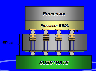
The picture to the right shows the basic architecture. On the top is the heatsinked processor die. There are no TSVs through the processor die. It is microbumped to attach to the memory die beneath it and to TSVs that go all the way through to carry the 200A of current that it requires direct from the package substrate. The processor/memory microbumps are at at a 50um pitch. The memory die to package bumps are 186um. The memory die has to be thinned in order to get the TSVs all the way through.

In addition, the memory die is choc-a-bloc with decoupling capacitors to reduce transient voltage droops. This allows for increased processor performance without having to give up area on the processor chip for the capacitors since they are in the metal on the memory die. At the keynote, there was a video showing the dramatic difference to the voltage across the chip with and without this approach to supplying power.

Posted in methodology, semiconductor | Comments Off

2½D: interposers

There are two classes of true 3D chips which are being developed today. The first is known as 2½D where a so-called silicon interposer is created. The interposer does not contain any active transistors, only interconnect (and perhaps decoupling capacitors), thus avoiding the issue of threshold shift mentioned above. The chips are attached to the interposer by flipping them so that the active chips do not require any TSVs to be created. True 3D chips have TSVs going through active chips and, in the future, have potential to be stacked several die high (first for low-power memories where the heat and power distribution issues are less critical).

The active die themselves do not have any TSVs, only the interposer. This means that the active die can be manufactured without worrying about TSV exclusion zones or threshold shifts. They need to be microbumped of course, since they are not going to be conventionally wire-bonded out. The picture at the head of this post shows (not to scale, of course) the architecture; click on the thumbnail for a larger image.

The image shows two die bonded to a silicon interposer using microbumps. There are metal layers of interconnect on the interposer, and TSVs to get through the interposer substrate to be able to bond with flip chip bumps to the package substrate. Flip-chip bumps are similar to micobumps but are larger and more widely spaced.

So is anyone using this in production yet? It turns out that Xilinx is using this for their Virtex-7 FPGAs. They call the technology “stacked silicon interconnect” and claim that it gives them twice the FPGA capacity at each process node. This is because very large FPGAs only become viable late after process introduction when a lot of yield learning has taken place. Earlier in the lifetime of the process, Xilinx have calculated, it makes more sense to create smaller die and then put several of them on a silicon interposer instead. It ends up cheaper despite the additional cost of the interposer because such a huge die would not yield economic volumes.

The Xilinx interposer consists of 4 layers of 65um metal on a silicon substrate. TSVs through the interposer allow this metal to be connected to the package substrate. Microbumps allow 4 FPGA die to be flipped and connected to the interposer. See the picture to the right. An additional advantage of the interposer is that it makes power distribution across the whole die simpler.

This seems to be the only design in high volume production, at least at the conference this was the example that every speaker seemed to use.

Posted in methodology, semiconductor | Comments Off

Going up: 3D ICs and TSVs

This is the first of several posts about 3D ICs. I attended the 3D architectures for semiconductor integration and packaging conference just before Christmas. I learned a lot but I should preface any remarks with the disclaimer that I’m not an expert on the subject, but I now know enough to be dangerous. But most people are not experts on this subject so I think it is worth a high level overview of what is happening.

The first thing is the 3D chips do seem to be happening. There are designs in production, there are lots of pilot projects and the ecosystem (in particular, who does what) seems to be starting to fall into place.

The first approach to talk about is flipping one chip and attaching it to the top of another. This is done by creating bonding areas on each chip, growing (usually copper) microbumps to create die-die interconnect at a pitch of approximately 50um. The big user of this technology is in digital camera chips. The CCD image sensor is actually thinned to the point that it is transparent to light and then attached to the image processing chip. The light from the camera lens passes through the silicon to the CCD unobstructed by interconnect etc which is all on the other side of the sensor.

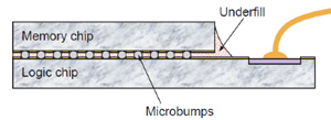
This approach is also used for putting a flipped memory chip onto a logic chip (see picture). It is not well-known, but the Apple A4 chip is built like this, with memory on top of the processor/logic chip. There are now standardization committees working on the pattern of microbumps to use for DRAMs (analagous to standard pinout for DRAMs) so that DRAM from different manufacturers should be interchangeable. Unlike in the picture, the bumps are all towards the center of the die so that the pattern is unaffected by the actual die size which may differ between manufacturers and between different generations of design.

Although this technology is formally 3D, since there are two chips, it doesn’t require any connections through any chips and is a sort of degenerate case.

You probably have heard that the key technology for real 3D chips is the through-silicon-via (TSV). This is a via that goes from the front side of the wafer (typically connecting to one of the lower metal layers) through the wafer and out the back. The TSV is typically about 5-10um across and goes about 8-10 times its width in depth, so 50-100um. A hole is formed into the wafer, lined with an insulator and then filled with copper. Finally the wafer is thinned to expose the backside. Note that this means that the wafer itself ends up 50-100um thick. Silicon is brittle so one of the challenges is handling wafers this thin both in the fab and when they have to be shipped to an assembly house. They need to be glued to some more robust substrate (glass or silicon) and eventually separated again during assembly. The wafer is thinned using CMP (chemical mechanical polishing, similar to how planarization is done between metal layers in a normal semiconductor process) until the TSVs are almost exposed. More silicon is then etched away to reveal the TSVs themselves.

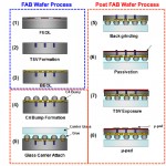
The picture to the right (click for a bigger image) shows Samsung’s approach. FEOL (which, for you designers, means front-end of line which means transistors and is nothing to do with front-end design) is done first. So the transistors are all created. Then the TSVs are formed. Then BEOL (which means back-end of line which means interconnect and is nothing to do with back-end design). After the interconnect is done then the microbumps are created. The wafer is glued to a glass carrier. The back is then ground down, a passivation layer is applied, this is etched to expose the TSVs and then micropads are created. This approach is known as TSVmiddle since the TSVs are formed between transistors and interconnect. There is also TSVfirst (build them before the transistors) and TSVlast (do them last and drill them through all the interconnect as well as the substrate).

There are two design issues with TSVs. First is the exclusion area around them. The via comes up through the active area and usually through some of the metal layers. Due to the details of manufacturing, quite a large area must be left around the TSV so that it can be manufactured without damaging the layers already deposited. The second problem is that the manufacturing process stresses the silicon substrate in a way that can alter the threshold values of transistors anywhere nearby, thus altering the performance of the chip in somewhat unpredictable ways.

Posted in methodology, semiconductor | Comments Off

Variation-aware Design

Solido has run an interesting survey on variation-aware design. The data is generic and not specific to Solido’s products although you won’t be surprised to know that they have tools in this area.

What is variation-aware design? Semiconductor manufacturing is a statistical process and there are two ways to handle this in the design world. One is to abstract away from the statistical detail into a pass/fail environment with concepts like minimum spacing rules and worst-case transistor timing. Meet the rules and the chip will yield. This is largely what we do in the digital world although with the complexity of modern design rules and the number of process corners that we now need to consider a lot of the complexity of the process is bleeding through anyway. But there is an underlying assumption in this approach that within-die variation is minimal. In fact the very idea of a process corner depends on this: all the n-transistors are at this corner and the p-transistors are at that corner.

But for analog this approach is no longer good enough, instead the design needs to be analyzed in the context of process variation for which the foundry needs to provide variation models. This requires statistical techniques in the tools to take the statistical data from the process and estimate its effect on yield, timing and power. It remains unclear to what extent these approaches will become necessary in the digital world as we move down the process nodes.

Solido had an agency survey several thousand IC designers of which nearly 500 completed the survey, so this is quite a large survey. They are a mixture of management and custom designers (so not digital designers).

The number #1 problem where they felt that advances were needed in tools were variation-aware design (66%) followed by parasitic extraction (48%). Coming up at the rear I don’t think anyone will be surprised that there isn’t a burning desire for major improvements in schematic capture (7%).

Of course the main reason people want variation-aware technology is to improve yield (74%) and avoid respins (64%) which is really just an extreme case of yield improvement! They also wanted to avoid project delays since over half of the groups had missed deadlines or had respins due to variation issues, typically causing a 2 month slip.

When asked which process node people though variation-aware design was important, surprisingly about 10% said that it was already important at 0.18µm, but that number is up to 60% by 65nm and 100% by 22nm.

So this is definitely something the analog guys need to worry about now, and digital need to be aware of. Indeed, Solido is part of the TSMC AMS reference flow (and other companies such as Springsoft and Synopsys have some variation-aware capabilities).

Posted in methodology, semiconductor | Comments Off

Magma’s new P&R and re-building the foundations

One of the important but often unrecognized aspects of engineering is re-building the infrastructure underneath key design tools. Sometimes this gives a new desirable capability but often a lot of the effort is simply to modernize the code base so that it is possible to continue development effectively going forward. For example, I remember in Compass days replacing our creaky graphics infrastructure with something more modern. It was expensive to do and it didn’t generate any additional revenue, but the old code had been written well over a decade before and was no longer adequate. Because this sort of infrastructure underlies everything, it is rather like changing the wheel of a car without stopping.

I met with Bob Smith of Magma late last year, and coincidentally I ran into Hamid Savoj, the CTO, at a conference on 3D chips a few days later. They have successfully done one of these changing the wheels without stopping exercises recently.

Magma’s engineering team have swapped out the old timing and extraction engines from Talus and replacing them with the Tekton timing engine and the QCP extraction engine to create Talus Vortex 1.2. This can place and route over one million cells per day with all the modern requirements for crosstalk, metal migration, multi-corner etc. It can handle up to 3M cells flat, which is important since probably one of the biggest wishes of the semiconductor customers is to be able to handle designs flat, or with as little hierarchy as they can get away with. Ideally today they would like to be able to handle 20 million cells or more flat. All hierarchy added in any design tool due to capacity limitations of the tool tends to cause design efficiency to drop, sometimes dramatically if the number of blocks grows large. But wait, there’s more, as the old ads say.

Along  with some further infrastructure work they have also created Talus Vortex FX which is the first distributed place and route solution. This pushes up the performance to over 3 million cells per day, and the capacity up above 8 million cells, which more than triples designer productivity. It analyzes the design, then partitions it into pieces that can be processed separately on their own server, and then eventually combines all the results back together (they call this Smart Sync). Some design tools are fairly easy to distribute (for example, DRC can be run on different parts of the chip in parallel and then stitched back together), some are very difficult (simulation, because there is a single global time-base so it is hard to find things that are independent) and some in between like place and route, although clever algorithms are needed to decide how to divide up the design amongst the computing resources.

As an irrelevant aside, in 1952 a car was driven across the US and back without stopping; of course it needed to have facilities to change a wheel without stopping. It can be seen today in the San Diego Automotive Museum.

Posted in eda industry, engineering | Comments Off

Carbon

In the latest piece that Jim Hogan and I put together about re-aggregation of value back at the system companies I talked a little bit about Carbon.

I got two things wrong, that I’d like to correct here. The first goes back a long way to the mergers of Virtutech, VaST and CoWare when I listed the other virtual platform companies that are still independent. I omitted Carbon since I didn’t actually realize they had acquired the virtual platform technology SOCdesigner from ARM when they did the deal to take responsibility for creating and selling ARM’s cycle accurate models.

SOCdesigner was originally a product from a company called Axys, based in southern California. I believe that they had technology pretty similar to VaST at the time, but it was hard to know since they were very secretive. Despite rules against doing so they would throw us out of their presentations at DAC and ESC (so we sent over our finance person to see what she could find out…but they even spotted her). ARM acquired Axys, which I never understood the reason for. Even ARM- based designs typically involve lots of models not from ARM, so it never seemed likely that ARM would be able to make SOCdesigner a successful standalone business, it seemed like a business for someone independent of the processor companies. After all, you can’t imagine MIPS putting much effort in to make their models run cleanly in SOCdesigner. At VaST we considered it less of a threat post-acquisition than before.

Anyway, Carbon got SOCdesigner (still called SOCdesigner) and used their own technology for turning RTL into fast C-based cycle accurate models to solve another problem ARM had, namely the cost of creating, maintaining and distributing cycle-accurate models. ARM had always had fast models of their processors and many peripherals, since that is what software developers required, and these are relatively cheap to produce (they only need to be functionally accurate so there are many corners that can be cut, for instance it is not usually necessary to model the cache or branch prediction since the only difference is the number of cycles used).

The second error was that I didn’t really realize that in the Carbon world there are now 3 speeds of models. RTL, cycle-accurate models, and fast models.

RTL models aren’t really in the Carbon world, actually. But cycle-accurate models are automatically generated from the RTL which means that they are correct by construction. These models are not fast enough for software development, and in fact it is impossible to create models that are fast enough for software development and simultaneously accurate enough for SoC development. However, given their RTL provenance they tie the software and the SoC design together accurately, which is really important because increasingly it is only possible to validate the software against the hardware and vice versa.

Fast models usually either come from the vendor of the processor or IP, or are created by the end-user. Processor models are not actually models in the usual sense of the word, they are actually just-in-time (JIT) compilers under the hood, converting instruction sequences from ARM, MIPS or whatever instructions into x86 instructions that run a full native speed. Fast peripheral models again are created by cutting lots of corners, but this is not something that can be done automatically since it is not clear (and often depends on the use to which the model will be put) which corners can be cut.

The remaining piece of the puzzle is the capability for the virtual platform to switch from fast models to cycle-accurate models. Boot up the system until it gets interesting (or perhaps just before to give the cycle-accurate models a bit of runway), then suck out all the state information from the fast models and inject into the cycle-accurate models. This gives the best of both worlds, fast models when you don’t care about the details of what is going on in the hardware, and complete accuracy when you do, either because you are responsible for verifying the hardware or debugging low-level software that interacts intimately with the hardware.

Posted in eda industry, methodology | Comments Off

Windows on ARM?

In a blog post last March I concluded:

My gut feel is that a mobile-internet-device will be more like a souped up smartphone than a dumbed down PC, and so Atom will lose to ARM. In fact I think the smartphone and MID markets will converge. Microsoft will lose unless they port to ARM.

Since I wrote that before the debut of the iPad, when lots of people wiser than me were holding the view that netbooks/tablets etc would all need to be Windows-compatible and thus Atom-based to be successful, I think it was a reasonably prescient view.

Yesterday, Bloomberg and the Wall Street Journal reported  that Microsoft is porting a version of Windows to ARM and will debut it at the Consumer Electronics Show in January. Of  course Windows Phone 7 already runs on ARM (specifically the Dragonball processor from Qualcomm) so Microsoft is not a complete stranger to ARM.

The WSJ article says that nothing will be available for two years, which, if true, makes saying anything at CES the ultimate pre-announcement. Indeed, it is a reasonable question to ask whether anyone will care by then. If Microsoft is going to have an ARM-based tablet operating system then I don’t think it can wait that long. Somehow in the mobile, smart-phone and tablet part of the market they never seem to miss an opportunity to miss an opportunity.

The likely loser in all of this is Intel and the winner is ARM and, if they produce something that gains market acceptance, Microsoft. With Windows on ARM, I think that the tablet (iPad-like) market will be largely ARM-based (just like smartphones) and Intel’s Atom processor will have a hard time gaining traction.

Posted in semiconductor | Comments Off

Evolution of design methodology, part II

The second half of the article that Jim Hogan and I wrote on re-aggregation of design at the system companies is now up at EEtimes.

The second part of the article looks at the implications for the EDA and IP industries of the changes that we outlined in the first part of the article.

Posted in eda industry, methodology | Comments Off

Pat Pistilli: the first cell library, the first printed label, and more

Pat Pistilli is this years Kaufman Award winner. I was out of the country for the award dinner so I didn’t attend but I talked to Pat earlier today.

Pat, who was at Bell Labs, started DAC (then called SHARE, the Society to Avoid Redundant Effort) 1964 along with a co-conspirator from IBM. The first conference was in Atlantic City in 1964. This eventually became DAC. When the availability of commercial EDA tools made DAC too big to manage as an all-volunteer organization as it had been, Pat left the technical side of design automation to form MP Associates along with his wife Marie. I think that the history of DAC has been well-covered elsewhere so instead, I asked Pat, what was “design automation” back when he started in the business. After all, transistors were fairly new, printed circuit boards hadn’t been invented, integrated circuits were in research and so on.

He told me about the design system he worked on, known as BLADES (for Bell LAbs DEsign System). It ran on an IBM704 with 32K of memory. Think about how little that is: 32 gigabytes (too big for a notebook but not for a high-end server)  is a million times as much. The computer had 32 tape-drives (disks were another thing that hadn’t yet been invented). They built the design system to work on a specific project, the Safeguard anti-missile system for the DoD. It was an electronic system so large it occupied 3 buildings.

The system was built like this. At the lowest level were modules which contained 3 or sometimes as many as, dramatic pause, 4 transistors with wire-wrap terminals (if you are too young to know what wire-wrap is, then more than you want to know is here). Boards 33″ by 24″ were covered in these modules with gaps in between to run the wires (because if you ran wires over  the tops of the modules you’d never be able to open them again for maintenance). Originally there were 8 different kinds of modules but eventually they ended up with about 30 (that sounds familiar in libraries today). Initially these modules were hard-wired into the code but Pat came up with the idea of putting all the components into a file on a magnetic tape and extracting them from there (the first cell-library I guess). The design rules, for example no wire could be longer than 12″, were on another tape.

These boards were stacked into refrigerator-sized units called frames with more wire-wrap to construct what today we’d call a back-plane. Then lots of these units would then be connected together with manually labeled wires until you’d filled 3 buildings.

Before Pat’s design automation it took 4-5 months to design one of these boards and then another month for the board to be wire-wrapped by hand. Afterward, using the design system, the time was cut to around a month but it still took another month for the hand wire-wrapping.

Then Gardner Denver developed an automatic wire-wrap machine. Pat designed a controller for this (complicated by the need for ‘dressing fingers’ since they couldn’t route point to point and had to avoid wires going over the modules). Now the design automation system could (effectively) directly manufacture the board. That got the time down from a month to a day or two.

This is one example of how manufacturing used to be much more connected to engineering, and delivering a system would often involve people needing to work in all sorts of areas. Software engineers today don’t have to change the design of the semiconductor manufacturing equipment!

The wires that connected the frames were manually labeled. But hand-written labels aren’t always legible, and the glue wasn’t good so they would regularly fall off leading to obvious problems. Pat decided they needed a new way of labeling where the labels could be printed automatically and would stick on the cables properly and never fall off. The only material he could find that seemed like a good starting point was the plastic sheet that 3M used to make band-aids. So he got band-aid material from 3M and would attach it to paper and print the labels using a standard line-printer. But the adhesive still wasn’t good enough so he got the chemical department at Bell Labs to invent a new super-strong adhesive and, further, to develop a coating for the plastic that would accept the ink (so it could be printed) but not dirt so the labels would stay clean and legible. They still needed 3M to supply the original plastic material and to do the die-cutting afterward. Finally, Pat modified a manual wire-wrap gun with a new chuck to create a tool that attached the labels to the wires, inspired by having seen cigarettes being made on a factory tour. These were the first ever machine-prepared labels.

3M actually branched off that part of the business to form a label-making subsidiary called Avery. Yes, the same Avery as makes labels for your inkjet today.

So what happened when three buildings worth of electronics was shipped out to an island in the Pacific? Safeguard was constructed because the US figured that they couldn’t build enough interceptors to destroy every incoming missile. But  they also figured out that the USSR couldn’t afford to build that many warheads so that they would use decoys too. Safeguard analyzed the incoming missile trajectories looking for tiny differences in flight path to decide which were real and which were decoys. Pat was invited out to the Pacific for the first test and it was a complete success. The system picked out the one real missile from the five decoys and knocked it down.

Interestingly, in the early days there were big problems getting acceptance of this new technology. Designers didn’t want to use the design system since they worried it would obstruct their creativity. And the manufacturing people were worried that the automation  would lose them their jobs. When Pat moved to Denver in 1969 it was the first time AT&T had both design and manufacturing under the same roof.  When he arrived the manufacturing manager told him “I hate computers.” Back then the design methodology was that Bell Labs would design the system and build prototypes, then the design would be transferred to Western Electric (the manufacturing arm) who would completely re-lay it out. With the design system this became unnecessary, the prototype could be transferred direct into manufacturing and this became a model for the rest of Western Electric. The system produced cost savings of $2M per year immediately. Since AT&T was a regulated utility, the only way for them to increase profitability was to reduce their costs since they didn’t really have any way to increase their prices. So this was a big deal and the manufacturing manager changed his tune.

Since DAC is 50 years old in a couple of years, I suggested that it would be interesting to have some other people talk about what design automation was in the 5 decades since it started. Now we are in the age of billion transistor chips it is hard to remember the time when 10,000 gates was a huge design, let alone all the automation necessary to create even earlier systems.
Posted in eda industry, engineering | Comments Off

30th Anniversary of Funding of VLSI Technology

Doug Fairbairn reminds me that today is the 30th anniversary of the funding of VLSI Techology. VLSI was really the first company to embrace the idea that integrated circuits could be designed by people outside the priesthood of the semiconductor companies themselves, what we now call IDMs. The original founders were Jack Baletto, Dan Floyd and Gunnar Wetlesen. Doug Fairbairn would become employee #4 when he went to interview the 3 of them for the infant VLSI Design Magazine (still called Lambda back then) and realized that they needed help in the software area if they were going to succeed as a manufacturing foundry, since there was no way to create a design with what was then available. This was the era when every semiconductor company developed its own tools and not long after the era when every semiconductor company developed its own manufacturing equipment.

The lead investors were Evans and Sutherland (the graphics and flight simulator company in Salt Lake City) and Hambrecht & Quist (one of the earlier VCs).

VLSI had an incredible, especially given its limited size, team of software engineers who put together an entire design system in a relatively short time. We were the first generation of PhDs who had learned the Mead-Conway methodology, so the first generation of computer-scientists rather than electrical engineers, who knew how to design a chip. For several years I think we had clearly the best design tools that you could buy. Of course you had to use VLSI to build your silicon to get your hands on them, which was a good business model when VLSI started out but became less tenable as the DMV (Daisy, Mentor, Valid) got going and promoted the idea of software coming from a 3rd party EDA industry with libraries as the link to manufacturing. When it was just DMV, largely used for simple gate-arrays, VLSI was still in good shape since more complex designs required more powerful tools. But when ECAD and SDA merged to form Cadence we suddenly had a whole lot more competition. Every semiconductor manufacturer, especially in Japan but even Intel (I bet you’d forgotten they were in ASIC for a while) entered the ASIC business.

Since they didn’t know what they were doing initially, they could only compete on price. In practice, they weren’t very competent for many years. We would often end up bidding on designs where our price (and LSI Logic’s, the other company founded at almost the same time focused on gate-arrays) were twice the Japanese. “Come back when they fail,” we’d say and usually they would.

I think it was Wilf Corrigan, CEO of LSI Logic, who pointed out that the EDA industry stole all the profit from ASIC. They shipped tools that, in the early days at least, really weren’t very good. But the ASIC manufacturers only made money when the design got through so they ended up incurring all the costs of support. If you look at VLSI Technology over the years, it made money some years, lost money other years but it never generated enough cash to grow organically when you took its capital requirements (we had 2 fabs) into account. At one point, as the ultimate vote of no-confidence in the ability to generate profit, VLSI’s book value was less than the cash in the bank.

I joined VLSI about 18 months later. I think my hire date was June 28th 1982 (and we all got a $100 bonus for July 4th that year, so not a bad start. $100 was worth something back then). I stayed for 16 years eventually sawing off the branch I was sitting on. By then I was running Compass and we were acquired by Avant! I stayed there for 8 hours after the deal finally closed, resigning on a Friday afternoon and starting at Ambit on Monday morning. Good decision.

The non-Compass part of VLSI was eventually acquired by Philips Semiconductors (now NXP) in a hostile takeover in 1999 for $1B.

By some measures, VLSI was a big success: we invented an industry, pioneered various design tools, were successful in PC chipsets, early into wireless and grew from nothing to a $600M (I think) business. But the stock price never went anywhere in 15 years, spending most of its time lingering in the $11 to $15 range. In fact from my personal financial point of view, the most important event was the 1987 stock market crash when all our options were repriced to $4. So once the stock went back to its usual range there was a nice profit.

But I learned an incredible amount about silicon, software development, management. Compared to most people in EDA I like to say I have silicon in my veins. I’m often disturbed by how little about semiconductors EDA people know. It was a great ride.

Posted in eda industry, investment, semiconductor | Comments Off